Pinning, Introduction, Functional description – Philips TEA1104T User Manual
Page 4: Mode latch, Supply block
1996 Feb 26
4
Philips Semiconductors
Objective specification
Cost effective battery monitor and fast
charge IC for NiCd and NiMH chargers
TEA1104; TEA1104T
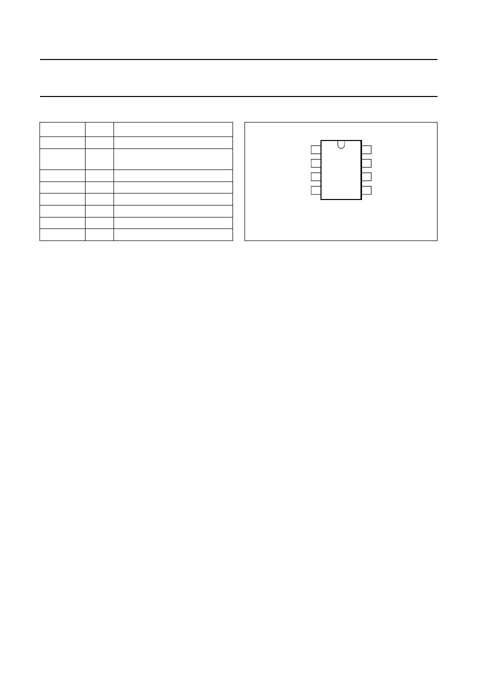
PINNING
SYMBOL
PIN
DESCRIPTION
GND
1
ground
NTC
2
negative temperature coefficient
resistor input
V
S
3
stabilized supply voltage
V
bat
4
battery voltage sensing
R
ref
5
reference resistor
V
P
6
positive supply voltage
OSC
7
oscillator input
LED
8
LED output
Fig.2 Pin configuration.
handbook, halfpage
1
2
3
4
8
7
6
5
MGE353
TEA1104
LED
OSC
NTC
VP
Rref
Vbat
Vs
GND
INTRODUCTION
The operation of the TEA1104; TEA1104T is explained
with the aid of the application diagram illustrated in Fig.7.
An application note (AN95085) is available describing the
versatility of the TEA1104; TEA1104T.
An external power current source charges the batteries via
an electronic switch which is controlled by the TEA1104.
The TEA1104 monitors the battery voltage. Fully charged
batteries are detected when the battery voltage peaks. In
fact, a voltage drop of 0.25% with respect to the top value
is detected. Fast charging is initiated at ‘power on’ or at
‘replaced batteries’. The switch is continuously on,
providing that all protection levels are met. At battery full
detection, the charge current is duty cycled to reduce the
average charge current to a lower level, keeping the
batteries fully charged but at he same time assuring long
battery life. In Fig.3 the battery voltage during fast charge
is plotted.
FUNCTIONAL DESCRIPTION
A block diagram of the TEA1104; TEA1104T is illustrated
in Fig.1
Mode latch
The Mode latch determines if the system is in the fast or in
the slow charge mode.
•
Fast charge is active at:
– power switch-on and battery connected
– temperature between minimum and maximum value
– battery insert
•
Trickle charge is active if:
– battery full is detected
– maximum time is exceeded
– maximum cut-off temperature is exceeded after the
initial phase.
Supply block
For correct start-up, the IC supply current is limited to
35
µ
A (typ.) until the start-up voltage of 6.4 V is reached
(standby mode). Thereafter, the operating supply voltage
V
P
has to be within the window of 5.45 to 11.5 V, meaning
that there is no need for an external voltage regulator to
supply the IC.
The supply block delivers the following outputs:
•
With the help of an external resistor (pin R
ref
), a
reference current is obtained which defines the
accuracy of all IC timing characteristics
•
Externally available 4.25 V stabilized voltage source
(V
source
). This source is used internally to supply a large
part of the circuit and can be used to set the NTC biasing
and to supply other external circuitry with a maximum
current of 1 mA. Protection information is provided via
V
S
, to design a dual LED indicator
•
Power-on reset pulse resets all digital circuitry after a
start or restart, due to an interrupted V
S
.