C-bus controlled yuv/rgb switch tda8443a – Philips TDA8443A User Manual
Page 9
1995 Mar 07
9
Philips Semiconductors
Product specification
I
2
C-bus controlled YUV/RGB switch
TDA8443A
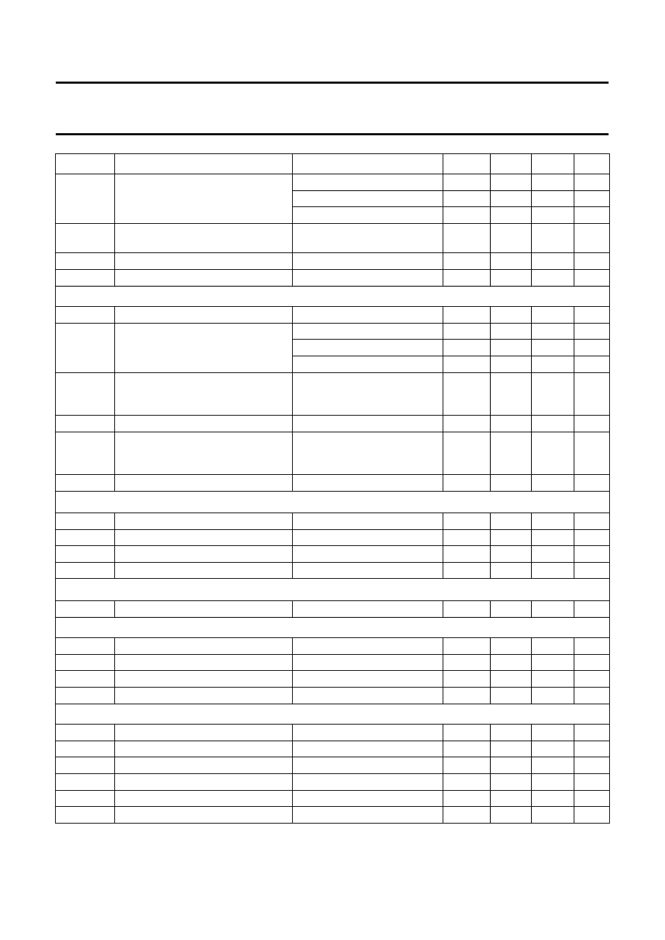
G
diff(p-p)
differential gain at nominal output
signals (peak-to-peak value)
R
−
Y = 1.05 V (p-p)
−
−
10
%
B
−
Y = 1.33 V (p-p)
−
−
10
%
Y = 0.34 V (p-p)
−
−
10
%
S/N
signal-to-noise ratio
nominal input; B = 5 MHz;
note 2
50
−
−
dB
SVRR
supply voltage ripple rejection
note 3
30
−
−
dB
V
O
DC output levels during clamping
−
5.3
−
V
Synchronization channels
G
diff
gain difference (programmed value)
−
−
10
%
B
bandwidth
−
3 dB
−
50
−
MHz
+3 dB; gain
×
1
−
20
−
MHz
±
3 dB; gain
×
2
−
13
−
MHz
V
i(p-p)
input amplitude of sync signal for
correct operation of clamp pulse
generator (peak-to-peak value)
0.2
−
2.5
V
|
Z
23-22
|
output impedance (pin 23)
−
20
30
Ω
V
o(p-p)
maximum undistorted output
amplitude (pin 23)
(peak-to-peak value)
2.5
−
−
V
V
O
DC output level on top of sync pulse
1.5
1.9
2.4
V
I
2
C-bus inputs for SDA, SCL
V
IH
HIGH level input voltage
3
−
V
P
V
V
IL
LOW level input voltage
−
0.3
−
1.5
V
I
IH
HIGH level input current
−
−
10
µ
A
I
IL
LOW level input current
−
−
10
µ
A
I
2
C-bus output for SDA (open collector)
V
OL
LOW level output voltage
I
OL
= 3 mA
−
−
0.4
V
Address selection inputs for S0, S1, S2
V
IH
HIGH level input voltage
3
−
V
P
V
V
IL
LOW level input voltage
−
0.3
−
0.4
V
I
IH
HIGH level input current
−
0
10
µ
A
I
IL
LOW level input current
−
50
−
10
0
µ
A
Fast switching input
V
IH
HIGH level input voltage
1
−
3
V
V
IL
LOW level input voltage
−
0.3
−
0.4
V
I
IH
HIGH level input current
−
0
500
µ
A
I
IL
LOW level input current
−
100
−
−
µ
A
t
sw
switching time
see Fig.5
−
10
−
ns
t
d
switching delay
see Fig.5
−
20
−
ns
SYMBOL
PARAMETER
CONDITIONS
MIN.
TYP.
MAX.
UNIT