Features, Description, Quick reference data – Philips CBT6800 User Manual
Page 2: Ordering information, Pin configuration, Pin description
Philips Semiconductors
Product data
CBT6800
10-bit bus switch with precharged outputs
for live insertion
2
2003 Sep 12
FEATURES
•
5
Ω
switch connection between two ports
•
TTL compatible input and output levels
•
Outputs are precharged by bias voltage to minimize signal
distortion during live insertion
•
Latch-up protection exceeds 100 mA per JESD78
•
ESD protection exceeds 2000 V HBM per JESD22-A114,
200 V MM per JESD22-A115 and 1000 V CDM per JESD22-C101
DESCRIPTION
The CBT6800 provides ten bits of high-speed TTL-compatible bus
switching. The low on-state resistance of the switch allows
bi-directional connections to be made while adding near-zero
propagation delay. The device also precharges the B port to a
user-selectable bias voltage (BIASV) to minimize live-insertion noise.
The CBT6800 is organized as one 10-bit switch with a single enable
(ON) input. When ON is low, the switch is on and port A is
connected to port B. When ON is high, the switch between port A
and port B is open and the B port is precharged to BIASV through
the equivalent of a 10 k
Ω
resistor.
The CBT6800 is characterized for operation from -40 to 85
°
C.
QUICK REFERENCE DATA
SYMBOL
PARAMETER
CONDITIONS
T
amb
= 25
°
C; GND = 0 V
TYPICAL
UNIT
t
PLH
t
PHL
Propagation delay
An to Bn or Bn to An
C
L
= 50 pF; V
CC
= 5 V
250
ps
C
IN
Input capacitance - control pin
V
I
= 0 V or V
CC
3.5
pF
C
OUT
Output capacitance - I/O pins
Outputs disabled; V
O
= 0 V or V
CC
8.2
pF
I
CCZ
Total supply current
Outputs disabled; V
CC
=5.5 V
1
µ
A
ORDERING INFORMATION
PACKAGES
TEMPERATURE RANGE
ORDER CODE
DWG NUMBER
24-Pin Plastic TSSOP
-40 to +85
°
C
CBT6800PW
SOT355-1
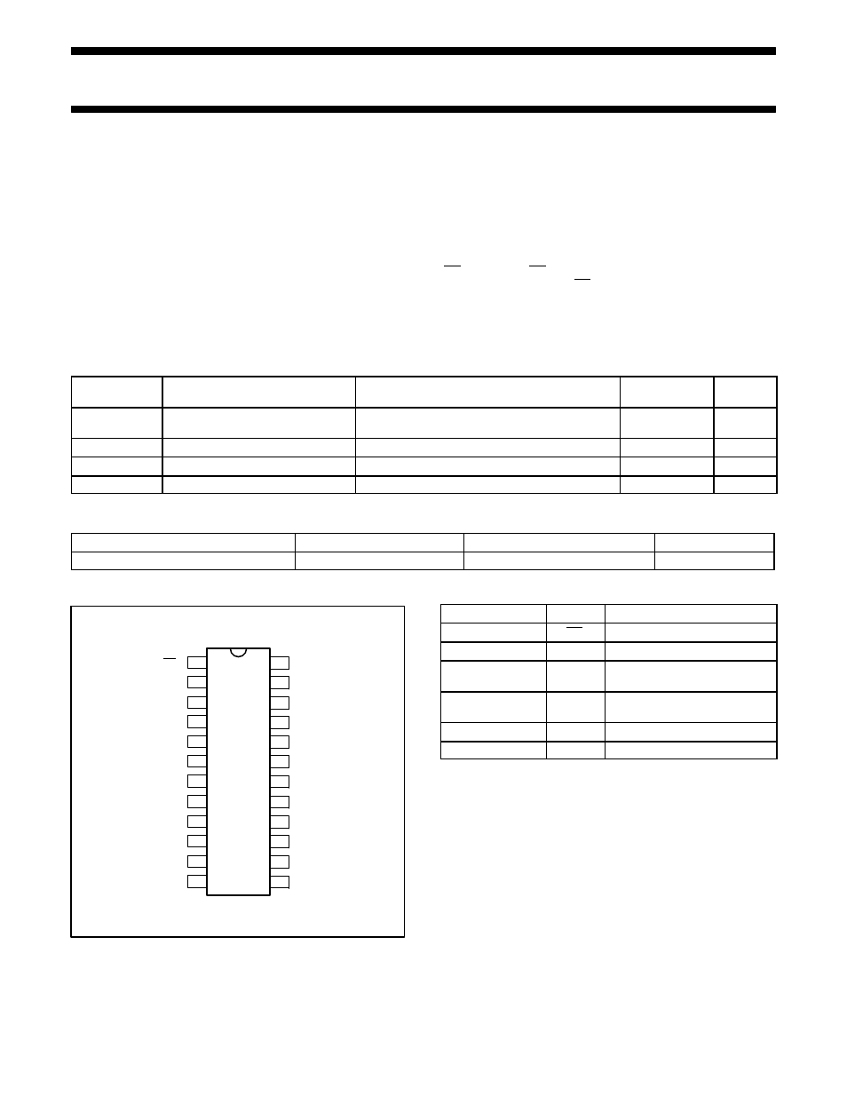
PIN CONFIGURATION
SA00505
1
2
3
4
5
6
7
8
9
10
11
12
24
23
22
21
20
19
18
17
16
15
14
13
A1
A2
A3
A4
A5
A6
A7
A8
A9
A10
GND
OE
Vcc
B1
B2
B3
B4
B5
B6
B7
B8
B9
B10
BIASV
PIN DESCRIPTION
PIN NUMBER
SYMBOL
NAME AND FUNCTION
1
OE
Output enable
13
BIASV
Precharge bias voltage input
2, 3, 4, 5, 6,
7, 8, 9, 10, 11
A1-A10
A-port I/O pins
23, 22, 21, 20, 19,
18, 17, 16, 15, 14
B1-B10
B-port I/O pins - with active pullup
12
GND
Ground (V)
24
V
CC
Positive supply voltage