SMSC USB2242 User Manual
Page 11
Ultra Fast USB 2.0 Memory Stick Flash Media Controller
Datasheet
SMSC USB2242/USB2242i
11
Revision 1.0 (05-27-08)
DATASHEET
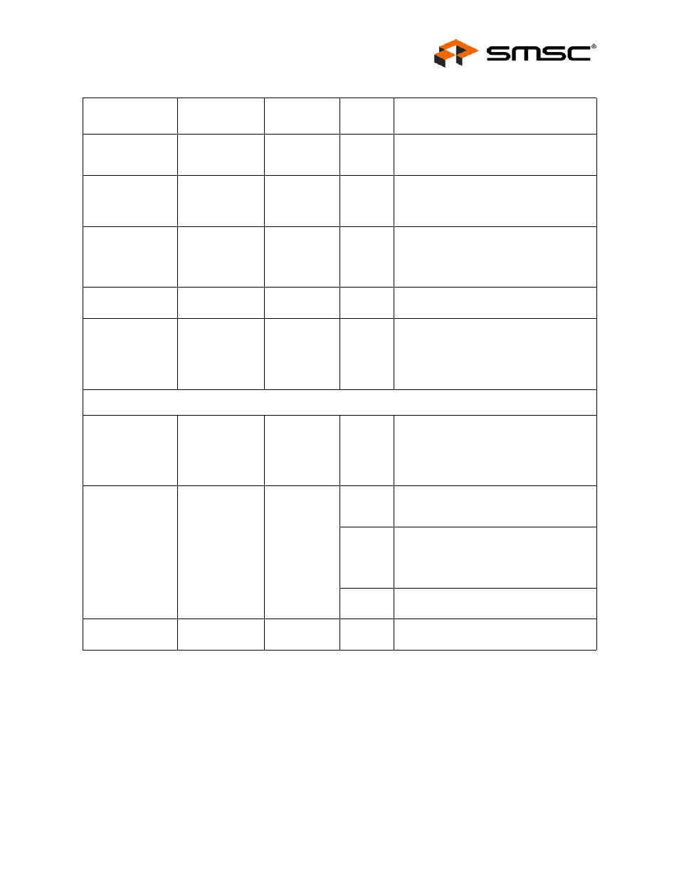
USB Transceiver
Bias
RBIAS
35
I-R
A 12.0k , 1.0% resistor is attached from
VSSA to this pin in order to set the
transceiver's internal bias currents.
24MHz Crystal or
external clock
input
XTAL1 (CLKIN)
33
ICLKx
This pin can be connected to one terminal
of the crystal or it can be connected to an
external 24 clock when a crystal is not
used.
24MHz Crystal
XTAL2
32
OCLKx
This is the other terminal of the crystal, or
it can be left open when an external clock
source is used to drive XTAL1(CLKIN). It
may not be used to drive any external
circuitry other than the crystal circuit.
3.3V Analog
Power
VDDA33
36
3.3V Analog Power
1.8V PLL Power
VDD18PLL
34
This pin is the 1.8V Power for the PLL.
+1.8V Filtered analog power for internal
PLL. This pin must have a 1.0
μ
F(or
greater) ±20% (ESR <0.1
Ω) capacitor to
VSS.
MISC
General Purpose
I/O
GPIO1 (LED1)
1
I/O12
This pin may be used either as input, edge
sensitive interrupt input, or output.
In addition, as an output, the GPIO1 can
use output controlled by the LED1_GPIO1
register.
General Purpose
I/O
GPIO2 / RXD /
SDA
27
I/O12
GPIO: This pin may be used either as
input, edge sensitive interrupt input, or
output.
I
RXD: In addition to the above, the signal
can be used as input to the RXD of UART
in the device, when the TXD_RXD_SEL
bit in UTIL_CONFIG1 register is cleared to
"0".
I/O12
SDA: This is the data pin when used with
an external serial EEPROM.
General Purpose
I/O
GPIO4
29
I/O12
This pin may be used either as input, edge
sensitive interrupt input, or output.
Table 5.2 USB2242/2242i 36-Pin QFN Pin Descriptions (continued)
NAME
SYMBOL
36-PIN QFN
BUFFER
TYPE
DESCRIPTION