Summit S93WD462 User Manual
Page 6
6
S93WD462/S93WD463
2029 2.2 1/23/01
SUMMIT MICROELECTRONICS, Inc.
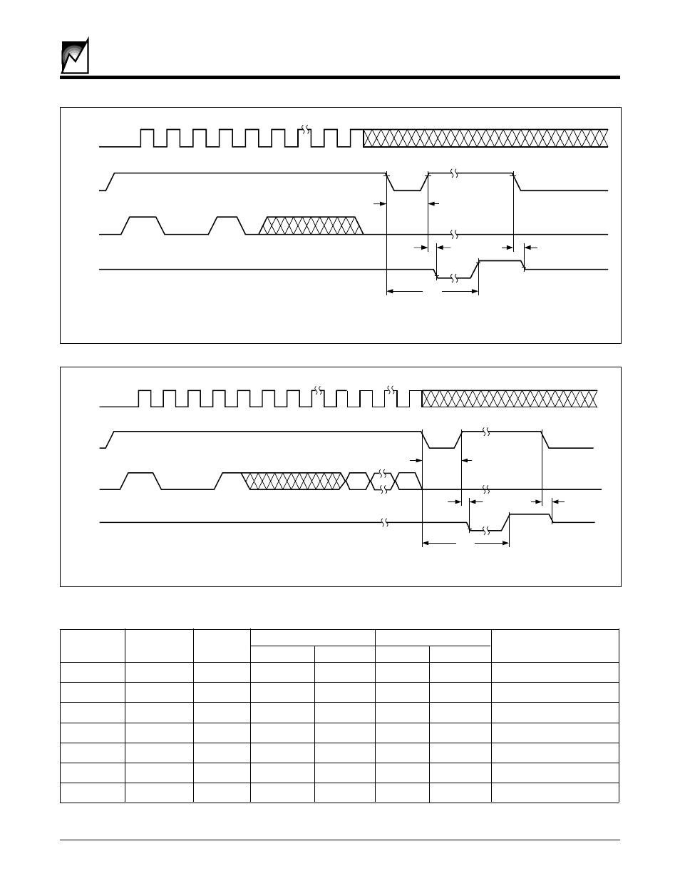
Figure 7. WRAL Instruction Timing
INSTRUCTION SET
Instruction
Start
Opcode
Address
Data
Comments
Bit
x8
x16
x8
x16
READ
1
10
A6–A0 A5–A0
Read Address AN–A0
ERASE
1
11
A6–A0 A5–A0
Clear Address AN–A0
WRITE
1
01
A6–A0 A5–A0 D7–D0 D15–D0
Write Address AN–A0
EWEN
1
00
11xxxxx
11xxxx
Write Enable
EWDS
1
00
00xxxxx
00xxxx
Write Disable
ERAL
1
00
10xxxxx
10xxxx
Clear All Addresses
WRAL
1
00
01xxxxx
01xxxx D7–D0 D15–D0
Write All Addresses
2029 PGM T5.0
Figure 6. ERAL Instruction Timing
SK
2029 ILL 8.0
CS
DI
DO
tCS
HIGH-Z
HIGH-Z
1
0
1
BUSY
READY
STATUS VERIFY
tSV
tHZ
t EW
0
0
STANDBY
SK
2029 ILL 10.0
CS
DI
DO
tCS
HIGH-Z
1
0
1
BUSY
READY
STATUS VERIFY
tSV
tHZ
t EW
0
0
STANDBY
D O
D N
This manual is related to the following products: