Pll circuits, Power supply circuits, 3 pll circuits – Icom IC-V8000 User Manual
Page 9: 4 power supply circuits

4 - 3
4-3
PLL CIRCUITS
4-3-1
PLL CIRCUIT (MAIN AND LOGIC UNITS)
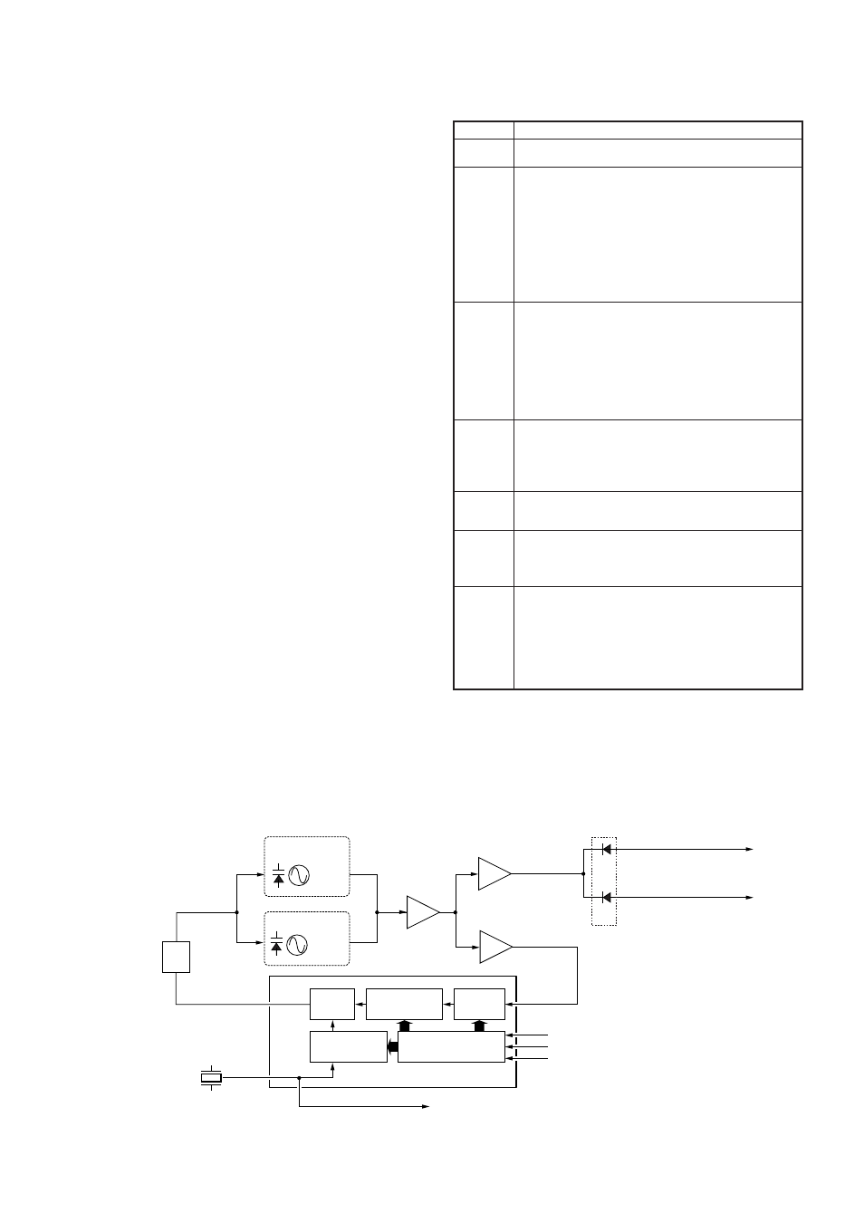
A PLL circuit provides stable oscillation of the transmit fre-
quency and receive 1st LO frequency. The PLL output com-
pares the phase of the divided VCO frequency to the refer-
ence frequency. The PLL output frequency is controlled by
the divided ratio (N-data) of a programmable divider.
An oscillated signal from the TX and RX-VCO circuits pass-
es through the LO and buffer amplifiers (Q9, Q12) is applied
to the PLL IC (IC1, pin 6) and is prescaled in the PLL IC
based on the divided ratio (N-data). The reference signal is
generated at the reference oscillator (X1) and is also applied
to the PLL IC. The PLL IC detects the out-of-step phase
using the reference frequency and outputs it from pin 15.
The output signal is passed through the loop filter(Q2) and
is then applied to the TX and RX-VCO circuits as lock volt-
age.
The lock voltage is also used for the receiver tunable band-
pass filters to match the filter’s center frequency to the
desired receive frequency. The lock voltage is passed
through the loop filter (Q2), and then applied to the DC
amplifier (Q10). The amplified signal is applied to the CPU
(LOGIC unit; IC7, pin 98) via the “LVIN” signal. The signal is
analyzed at the CPU, and then applied to bandpass filters
(D9–D11, D13) as “T1”, “T2”, “T3” signals via the D/A con-
verter.
4-3-2
VCO CIRCUIT (MAIN UNIT)
The VCO circuit contains a separate TX-VCO (Q6, D2, D4)
and RX-VCO (Q7, D5). The oscillated signal is amplified at
the LO (Q9) and buffer (Q11) amplifiers, and is then Tx/Rx
switching circuit (D6, D7). Then Tx and Rx signals are
applied to the pre-driver (Q17) and 1st mixer circuit (Q19)
respectively.
A portion of the signal from LO amplifier (Q9) is amplified at
the buffer amplifier (Q12) and is then fed back to the PLL IC
(IC1, pin 6) as the comparison signal.
Shift register
Prescaler
Phase
detector
Loop
filter
Programable
divider
Reference
divider
X1
25.25 MHz
Q6,
D2,
D4
TX VCO
RX VCO
LO
D7
D6
Q12
Q9
Q2
2
3
4
PLLCK
IC1 (PLL IC)
PLLDATA
PLLSTB
to transmitter circuit
to 1st mixer circuit (Q19)
1
9
6
Q7,
D5
Buff.
Q11
TX/RX
switch
Buff.
25.25 MHz 2nd LO signal
to the 2nd IF IC (IC4, pin 2)
• PLL CIRCUIT
LINE
HV
SWHV
C5V
+8V
+5V
T8
R5V
DESCRIPTION
The voltage from the power supply.
The same voltage as HV line which is controlled
by the HVSW circuit (Q28, Q30, Q31). When the
[POWER] switch is pushed, the CPU outputs the
“PWRON” control signal via the expander IC
(IC2). The signal is applied to the HVSW circuit
to turn the circuit ON.
The output voltage is applied to the drive ampli-
fier (Q18), +8V regulator circuit (IC7), etc.
Common 5 V for the CPU converted from the HV
line by the C5V regulator circuit (IC8). The circuit
outputs the voltage regardless of the power
ON/OFF condition.
The output voltage is applied to the EEPROM
(LOGIC UNIT; IC5), CPU (LOGIC UNIT; IC7),
etc.
Common 8 V converted from the 13.8 V line by
the +8V regulator circuit (IC7).
The output voltage is applied to the LO (Q9) and
buffer (Q11) amplifiers, etc.
Common 5 V converted from the +8 V line by the
+5V regulator circuit (Q21, Q22).
Transmit 8 V controlled by the T8V regulator cir-
cuit (Q14, Q15) using the “TXC” signal from the
I/O expander IC (IC2).
Receive 5 V controlled by the R5V regulator cir-
cuit (Q25) using “RXC” signal from the I/O
expander IC (IC2).
The output voltage is applied to the FM IC IC
(IC4), IF (Q16) and RF (Q27) amplifiers, etc.
4-4
POWER SUPPLY CIRCUITS
VOLTAGE LINE
