Pin assignments, Mb15f74ul – FUJITSU MB15F74UL User Manual
Page 2
MB15F74UL
2
(Continued)
• Direct power saving function : Power supply current in power saving mode
Typ 0.1
µ
A (V
CC
=
Vp
=
3.0 V, Ta
=
+
25
°
C)
Max
10
µ
A (V
CC
=
Vp
=
3.0 V)
• Software selectable charge pump current : 1.5 mA/6.0 mA Typ
• Dual modulus prescaler : 4000 MHz prescaler (64/65 or128/129) /2000 MHz prescaler (32/33 or 64/65)
• 23 bit shift register
• Serial input binary 14-bit programmable reference divider : R
=
3 to 16,383
• Serial input programmable divider consisting of:
- Binary 7-bit swallow counter : 0 to 127
- Binary 11-bit programmable counter : 3 to 2,047
• Built-in high-speed tuning, low-noise phase comparator, current-switching type constant current circuit
• On-chip phase control for phase comparator
• On-chip phase comparator for fast lock and low noise
• Built-in digital locking detector circuit to detect PLL locking and unlocking
• Operating temperature : Ta
=
−
40
°
C to
+
85
°
C
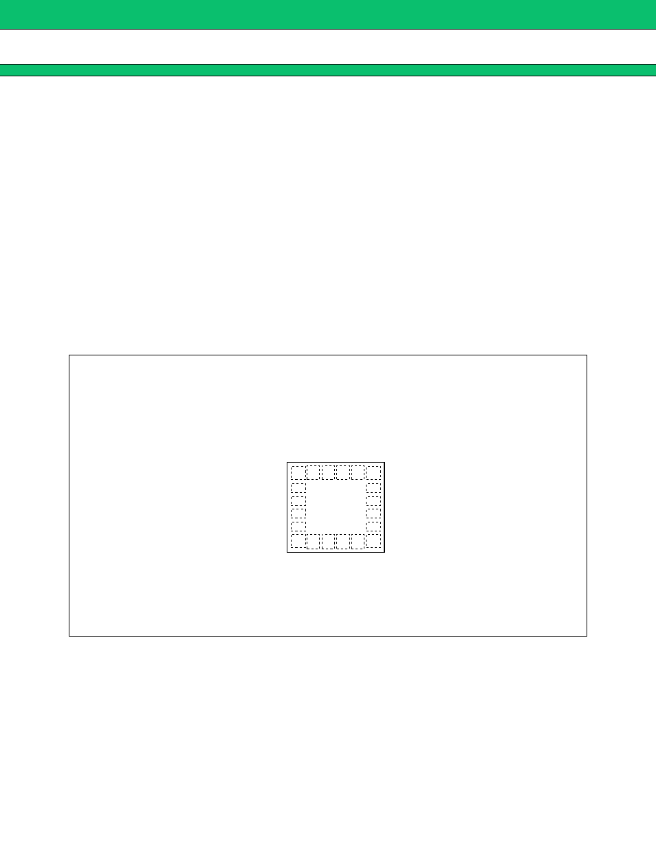
■
PIN ASSIGNMENTS
(BCC-20)
TOP VIEW
(LCC-20P-M05)
fin
IF
Xfin
IF
GND
IF
V
CCIF
PS
IF
Vp
IF
1
2
3
4
5
6
16
15
14
13
12
11
LE
fin
RF
Xfin
RF
GND
RF
V
CCRF
PS
RF
7
8
9
10
20 19 18 17
Do
IF
Do
RF
LD/fout
Vp
RF
GND
OSC
IN
Data
Clock