Fujitsu microelectronics america, inc – FUJITSU CS90A User Manual
Page 2
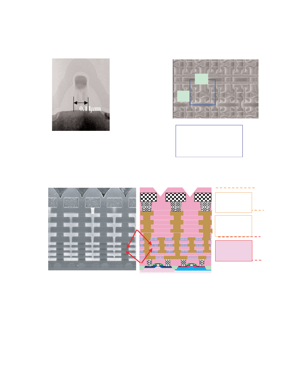
130nm node CMOS Process (CS90A)
Al
5-Cu
6-Cu
7-Cu
1-Cu
2-Cu
3-Cu
4-Cu
SiLK
SiO2
Al
Global Metal:
AL (Fuse & Pad)
Pitch: 1.8
µm
Semi Global Metal:
Thick Cu + SiO2
Pitch: 0.6
µm
Intermediate Metal:
Thin Cu + SiLK
Pitch: 0.4
µm
SRAM
Transistor
Interconnect
©2003 Fujitsu Microelectronics America, Inc.
All company and product names are trademarks or
registered trademarks of their respective owners.
Printed in the U.S.A. WFS-FS-20983-7/2003
FUJITSU MICROELECTRONICS AMERICA, INC.
Corporate Headquarters
1250 E. Arques Ave. Sunnyvale, CA 94088-3470
Tel: (800) 866-8608 Fax: (408) 737-5999
E-mail: [email protected] Web Site: http://www.fma.fujitsu.com
Cell Size =
1.98µm
2
(1.2µm x 1.65µm)
(2nd Generation SRAM)
1.65µm
See also other documents in the category FUJITSU Hardware:
- XG Series P3NK-4452-01ENZD (614 pages)
- FPCAC14C (1 page)
- MCJ3230SS (161 pages)
- MBA3073NC (138 pages)
- T5140 (102 pages)
- T5140 (76 pages)
- MAM3367MC/MP (152 pages)
- MPC3045AH (185 pages)
- MB2142-02 (23 pages)
- MB15F86UL (6 pages)
- MHS2030AT (40 pages)
- MHW2100BS (296 pages)
- MHK2060AT (227 pages)
- Disk Drives MHK2060AT (227 pages)
- MCM3064SS (170 pages)
- Mainboard D1561 (45 pages)
- MHC2040AT (219 pages)
- D1961 (45 pages)
- DISK DRIVES MHM2100AT (231 pages)
- MHR2010AT (250 pages)
- MHZ2120BJ (320 pages)
- MCE3064AP (175 pages)
- LQFP-64P (16 pages)
- Solaris PCI GigabitEthernet 3.0 (115 pages)
- MAY2036RC (94 pages)
- MAB3091 (142 pages)
- MPE3XXXAT (191 pages)
- MHV2040AH (40 pages)
- MHW2040AC (278 pages)
- ETERNUSmgr P2X0-0202-01EN (64 pages)
- VSS Hardware Provider 2.1 (134 pages)
- MAG3182FC (61 pages)
- MAU3147NC/NP (130 pages)
- MAX3147RC (94 pages)
- MHV2160BT (296 pages)
- MHV2040AT (280 pages)
- MAW3300NC/NP (130 pages)
- DeskPower E623 (50 pages)
- MAG3182LC (133 pages)
- OPTICAL DISK DRIVES MDG3064UB (42 pages)
- MHF2021AT (225 pages)
- MHR2040AT (40 pages)
- Single Drive FTM7926FB (1 page)
- PG-FCS103 (98 pages)
- MAS3735FC (114 pages)