Electrical characteristics, Mb3887 – FUJITSU MB3887 User Manual
Page 8
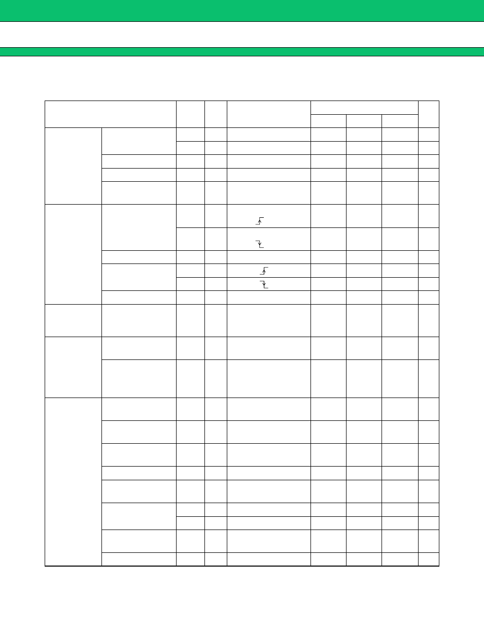
MB3887
8
■
ELECTRICAL CHARACTERISTICS
(Ta
=
+
25
°
C, VCC
=
19 V, VCC (O)
=
19 V, VREF
=
0 mA)
* : Standard design value.
(Continued)
Parameter
Sym-
bol
Pin
No.
Conditions
Value
Unit
Min
Typ
Max
1.
Reference
voltage block
[REF]
Output voltage
V
REF1
6
Ta
=
+
25
°
C
4.967
5.000
5.041
V
V
REF2
6
Ta
=
−
10
°
C to
+
85
°
C
4.95
5.00
5.05
V
Input stability
Line
6
VCC
=
8 V to 25 V
3
10
mV
Load stability
Load
6
VREF
=
0 mA to
−
1 mA
1
10
mV
Short-circuit output
current
Ios
6
VREF
=
1 V
−
50
−
25
−
12
mA
2.
Under voltage
lockout protec-
tion circuit
block
[UVLO]
Threshold voltage
V
TLH
18
VCC
=
VCC (O) ,
VCC
=
6.2
6.4
6.6
V
V
THL
18
VCC
=
VCC (O) ,
VCC
=
5.2
5.4
5.6
V
Hysteresis width
V
H
18
VCC
=
VCC (O)
1.0*
V
Threshold voltage
V
TLH
6
VREF
=
2.6
2.8
3.0
V
V
THL
6
VREF
=
2.4
2.6
2.8
V
Hysteresis width
V
H
6
0.2
V
3.
Soft-start block
[SOFT]
Charge current
I
CS
22
−
14
−
10
−
6
µ
A
4.
Triangular
waveform os-
cillator circuit
block
[OSC]
Oscillation
frequency
f
OSC
20
RT
=
47 k
Ω
260
290
320
kHz
Frequency
temperature
stability
∆
f/fdt
20
Ta
=
−
30
°
C to
+
85
°
C
1*
%
5-1.
Error amplifier
block
[Error Amp1,
Error Amp2]
Input offset voltage
V
IO
3, 4,
8, 9
FB1
=
FB2
=
2 V
1
5
mV
Input bias current
I
B
3, 4,
8, 9
−
100
−
30
nA
In-phase input
voltage range
V
CM
3, 4,
8, 9
0
V
CC
−
1.8
V
Voltage gain
A
V
5, 7 DC
100*
dB
Frequency
bandwidth
BW
5, 7 AV
=
0 dB
2*
MHz
Output voltage
V
FBH
5, 7
4.7
4.9
V
V
FBL
5, 7
20
200
mV
Output source
current
I
SOURCE
5, 7 FB1
=
FB2
=
2 V
−
2
−
1
mA
Output sink current
I
SINK
5, 7 FB1
=
FB2
=
2 V
150
300
µ
A