Chapter 3, Board layout – Lanner VES-8X6 User Manual
Page 14
14
Board Layout
Chapter 3
Embedded and Industrial Computing
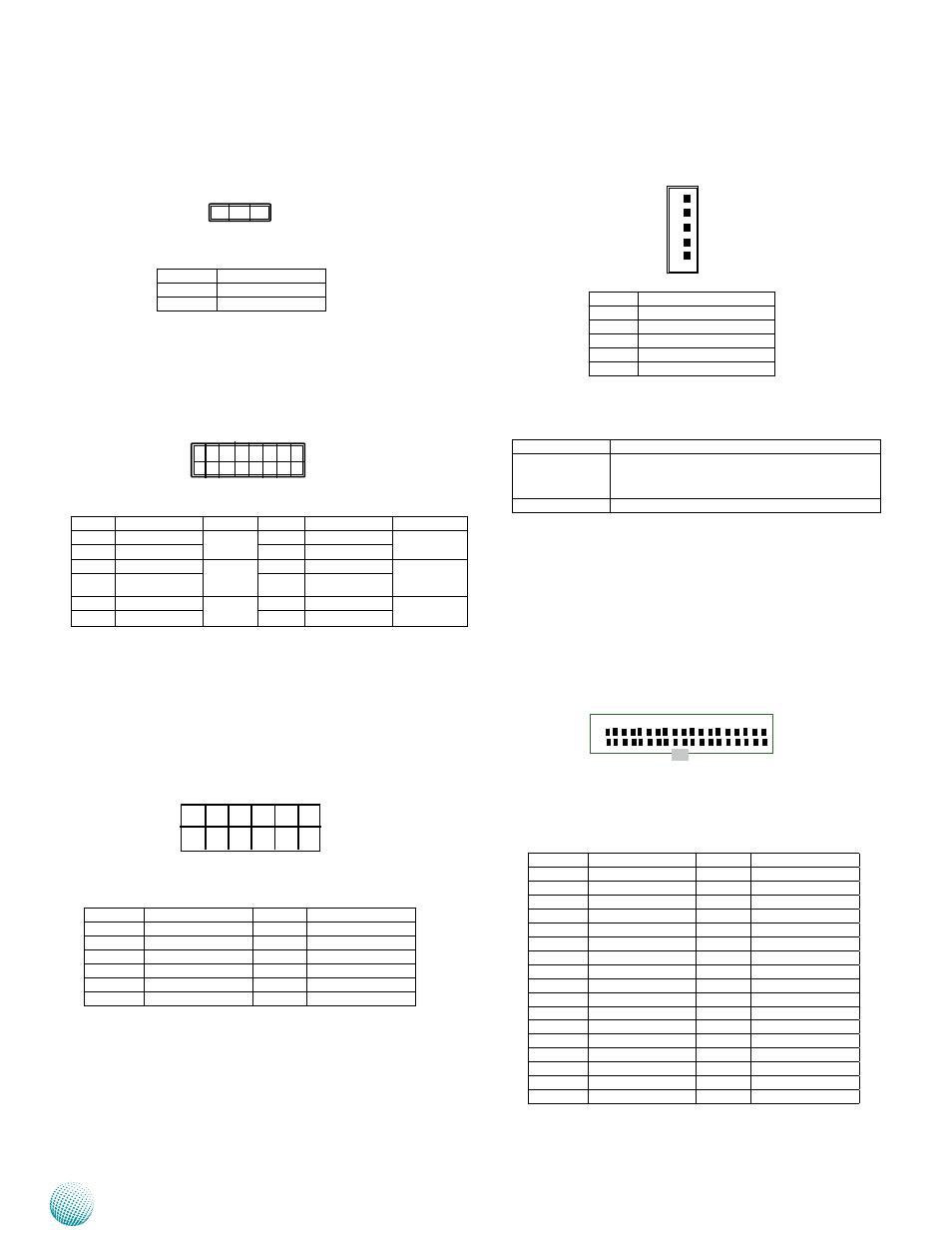
Clear CMOS (JBAT1)
Front Panel Connector (JFP1)
Multi-purpose Connector (JCN3)
Pin No.
Signal
1-2
Normal (default)
2-3
Clear CMOS
Pin No.
Signal
Function Pin No.
Signal
Function
1
EXT_PWRBTN#
Power
Button
7
+5V
HDD LED
2
GND
8
SATA_LED#
3
SYS_RERST#
Reset
9
EXT_PWRBTN# Short = AT
Open = ATX
4
GND
10
AT_BN
5
+5V
Power
LED
11
CASEOPEN#
Case Open
6
GND
12
GND
LCD Inverter Connector (JBKL1)
Signal Description of JBKL1
Floppy connector (FDC1)
1
2
5
Pin No.
Signal
1
+12V_BKL
2
GND
3
BKLEN
4
LVDS_BKLT_CTRL/PWM
5
+5V
Signal
Function
LVDS_BKLT_CTRL when LVDS_BKLT_CTRL is controlled by JVR1
header, Vadj = 0.75V ~ 4.25V (Recommended:
4.7KΩ, >1/16W)
BKLEN
LCD backlight ON/OFF control signal
2
1
Pin No.
Signal
Pin No.
Signal
1
GND
2
DRVDEN0
3
GND
4
NC
5
6
NC
7
GND
8
INDEX#
9
GND
10
MOA#
11
GND
12
NC
13
GND
14
DSA#
15
GND
16
NC
17
GND
18
DIR#
19
GND
20
STEP#
21
GND
22
WD#
23
GND
24
WE#
25
GND
26
TRAK0#
27
GND
28
WP#
29
GND
30
RDATA#
31
GND
32
HEAD#
33
GND
34
DSKCHG#
3 2 1
1
Pin No.
Signal
Pin No.
Signal
1
SER0_TX
2
SER0_RX
3
SER1_TX
4
SER1_RX
5
SLEEP#
6
GND
7
LID#
8
GND
9
PP_TPM
10
GND
11
PP_TPM
12
+3VSB
2
1