Rainbow Electronics MAX9508 User Manual
Page 2
MAX9508
Video Filter Amplifier with SmartSleep and
Bidirectional Video Support
2
_______________________________________________________________________________________
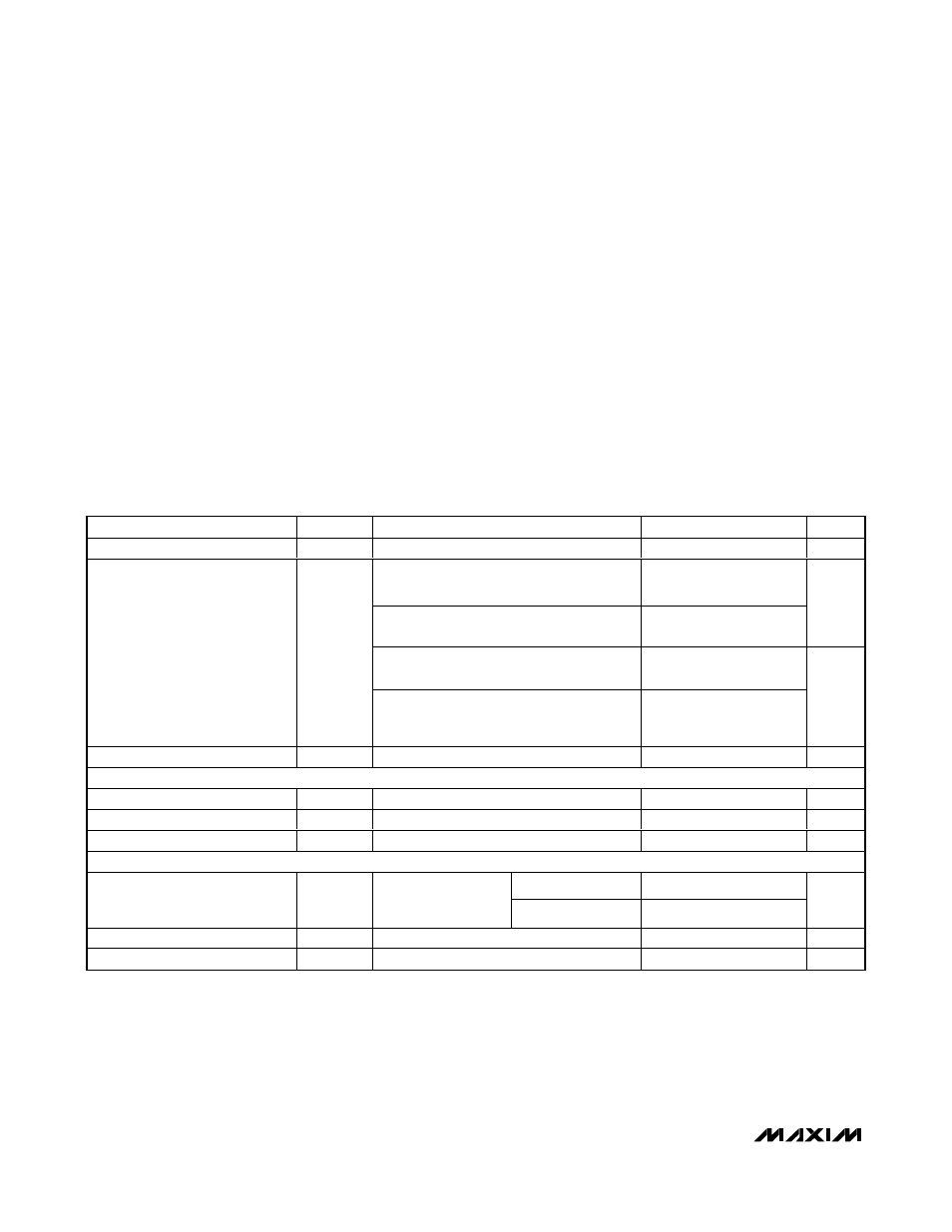
ABSOLUTE MAXIMUM RATINGS
ELECTRICAL CHARACTERISTICS
(V
DD
= V
SHDN
= 3.3V, V
SMARTSLEEP
= V
INT/EXT
= GND = 0V, R
L
= No load. T
A
= T
MIN
to T
MAX
, unless otherwise noted. Typical val-
ues are at T
A
= +25°C.) (Note 1)
Stresses beyond those listed under “Absolute Maximum Ratings” may cause permanent damage to the device. These are stress ratings only, and functional
operation of the device at these or any other conditions beyond those indicated in the operational sections of the specifications is not implied. Exposure to
absolute maximum rating conditions for extended periods may affect device reliability.
(Voltages with respect to GND.)
VDD ..........................................................................-0.3V to +4V
SMARTSLEEP, SHDN, INT/EXT
CIN, YIN, CVBSIN, EXTCVBSIN ..........................-0.3V to +4V
Duration of COUT, YOUT, CVBSOUT1, CVBSOUT2
Short Circuit to VDD or GND ..................................Continuous
Continuous Input Current
(CIN, YIN, EXTCVBSIN, CVBSIN,
SMARTSLEEP, SHDN, INT/EXT)...................................±20mA
Continuous Power Dissipation (TA = +70°C)
16-Pin TQFN (derate 15.6mW/°C above +70°C)..........1250mW
16-Pin QSOP (derate 8.3mW/°C above +70°C)...........667mW
Operating Temperature Range .........................-40°C to +125°C
Junction Temperature ......................................................+150°C
Storage Temperature Range .............................-65°C to +150°C
Lead Temperature (soldering, 10s) .................................+300°C
PARAMETER
SYMBOL
CONDITIONS
MIN
TYP
MAX
UNITS
Supply Voltage Range
V
DD
Guaranteed by PSRR
2.7
3.6
V
INT/E X T = G N D ( 4 channel s acti ve) ,
YIN = CVBSIN = 0.3V, CIN = 0.6V
13
16
INT/EXT = V
DD
(1 channel active),
EXTCVBSIN is unconnected
4.3
6
mA
SMARTSLEEP = V
DD,
CVBSIN has no active video signal
7
14
Supply Current
I
DD
SMARTSLEEP = V
DD
, CVBSIN has a black-
burst video signal with sync tip at GND
(Note 2)
17
µA
Shutdown Supply Current
I
SHDN
V
SHDN
= GND
0.01
10
µA
SMARTSLEEP CHARACTERISTICS
Minimum Line Frequency
CVBSIN
14.3
kHz
Sync Slice Level
CVBSIN
4.1
5.2
% V
DD
Output Load Detect Threshold
Sync pulse present, R
L
to GND
200
Ω
DC CHARACTERISTICS
2.7V < V
DD
< 3.6V
0
1.05
Input-Voltage Range
V
IN
C IN , Y IN , C V BS IN ,
g uar anteed b y outp ut
vol tag e sw i ng
3.0V < V
DD
< 3.6V
0
1.2
V
Input Current
I
IN
CIN = YIN = CVBSIN = 0V
2
5
µA
Input Resistance
R
IN
CIN, YIN, CVBSIN
20
M
Ω