7 typical application diagram tfa9810, Tfa9810, Nxp semiconductors – NXP Semiconductors TFA9810 User Manual
Page 22: Audio amplifier 2 x 12 w
TFA9810_3
© NXP B.V. 2008. All rights reserved.
Product data sheet
Rev. 03 — 20 February 2008
22 of 29
NXP Semiconductors
TFA9810
Audio amplifier 2 x 12 W
14.7 Typical application diagram TFA9810
The typical application diagram with the TFA9810 supplied from an asymmetrical supply is
shown in
.
V
P
= 12 V, R
L
= 8
Ω
, P
o
= 1 W
(1) OUT1
(2) OUT2
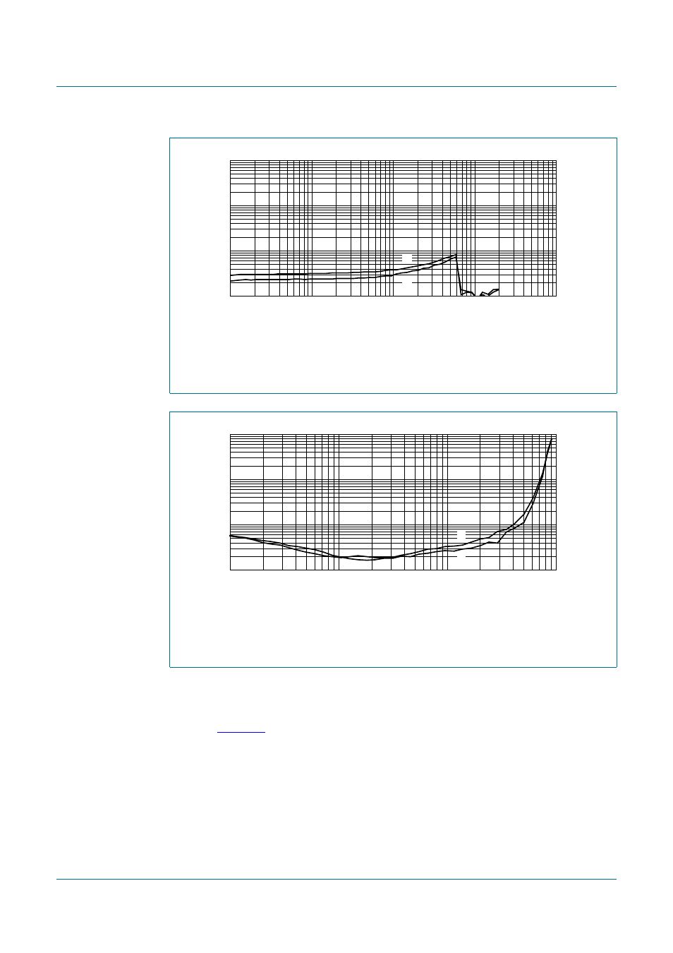
Fig 31. Total harmonic distortion + noise as a function of frequency
V
P
= 12 V, R
L
= 8
Ω
, f
i
= 1 kHz
(1) OUT1
(2) OUT2
Fig 32. Total harmonic distortion as a function of output power
010aaa195
f
i
(Hz)
10
10
5
10
4
10
2
10
3
1
10
−
1
10
THD+N
(%)
10
−
2
(1)
(2)
010aaa196
P
o
(W)
10
−
2
10
1
10
−
1
1
10
−
1
10
THD+N
(%)
10
−
2
(1)
(2)