4 3 volt operation, 10 reset switch, 11 clock source – Freescale Semiconductor Demonstration Board DEMO9S08AC60E User Manual
Page 16: 12 rs-232, Table 1-6 rs-232 connections, 3 volt operation, Reset switch, Clock source, Rs-232, Rs-232 connections

DEMO9S08AC60E User’s Guide, Rev. 0.1
16
Freescale Semiconductor
1.9.4 3 Volt Operation
The DEMO9S08AC60E can be run with VDD set to either 5 volts or 3 volts. To
run the board at 3V when using any of the three power options, move jumper
W1 to the 1-2, 3V position.
1.10 Reset Switch
The reset switch (SW6) provides a way to apply a reset to the MCU. The reset
switch is connected directly to the RESET_B signal of the MCU. A 10K pull up
resistor to VDD on the RESET_B signal allows for normal operation. When the
reset switch is pressed the RESET_B signal is grounded and the MCU
recognizes a reset.
1.11 Clock Source
An on-board 4MHz crystal (Y1) is connected between the XTAL and EXTAL
pins of the MCU. There is also an option for the user to add a canned oscillator
to the board. To add an oscillator, the zero ohm resistors R18 and R20 should
be removed and an oscillator should be installed in the J2 footprint. This
footprint accepts either 14 pin or 8 pin oscillators. To go back to the crystal
option, the oscillator should be removed from J2 and zero ohm resistors should
be reinstalled in the R18 and R20 footprints.
1.12 RS-232
An RS-232 translator provides RS-232 communication on com connector J34.
This connector is a 9 pin Dsub right angle connector. TXD and RXD signals are
routed from the MCU to the RS-232 transceiver.
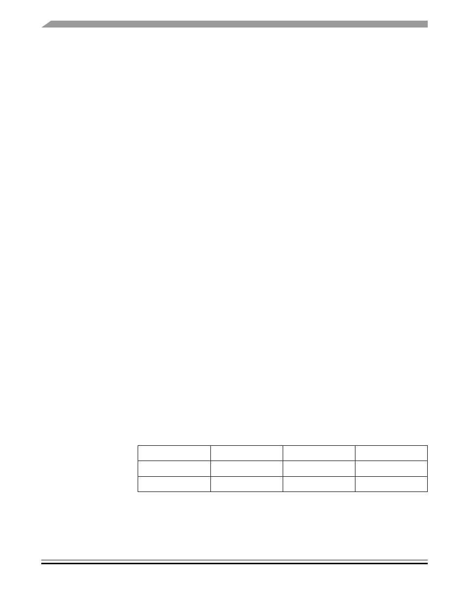
Table 1-6 RS-232 Connections
MCU Port
Jumper
COM Signal
I/O Port Connector
PTE0/TXD1
J14
TXD OUT
J34-2
PTE1/RXD1
J15
RXD IN
J34-3
To disconnect port pins PTE0 and PTE1 from the RS-232 translator, remove
jumpers J14 and J15. The full pinout of the COM connector (J34) is listed below
