Decoder operation, Setting the receiver address, The data outputs – Linx Technologies RXD-xxx-KH2 User Manual
Page 4: Receiving data, Power supply requirements
Page 7
Page 6
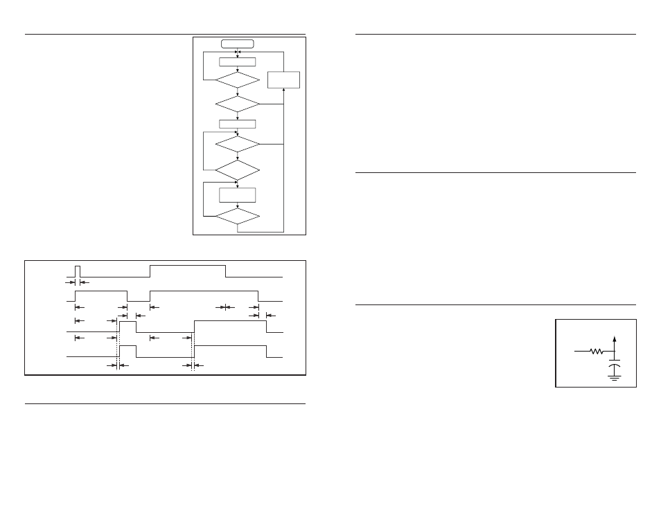
DECODER OPERATION
The KH2 Series receiver utilizes the HT658
decoder from Holtek. The decoder receives
data transmitted by the encoder and
interprets the first 10 bits of the code period
as address and the last 8 bits as data. A
signal on the DATA line activates the
oscillator, which in turn decodes the
incoming address and data. The decoder
will check the received address twice
continuously. If the received address code
matches the decoder’s local address, the 8
bits of data are replicated on the output
lines, and the VT line is set high to indicate
the reception of a valid transmission. That
will last until the address code is incorrect or
no signal has been received. The VT line is
high only when the transmission is valid,
otherwise it is low. The data outputs are
momentary, and follow the encoder during a
valid transmission, then reset.
The oscillator is disabled in the standby
state and activated as long as a logic “high”
signal is applied to the DATA line, so the
DATA line should be kept “low” if there is no signal input.
SETTING THE RECEIVER ADDRESS
The module provides ten tri-state address lines. This allows for the formation of
up to 59,049 (3
10
) unique receiver-transmitter relationships. Tri-state means that
the address lines can be set to one of three distinct states: high, low, or floating.
These lines may be hardwired or configured via a microprocessor, DIP switch,
or jumpers.
The receiver’s address line states must match the transmitter’s exactly for a
transmission to be recognized. If the transmitted address does not match the
receiver’s local address, then the receiver will take no action.
Power On
Standby Mode
Code In?
No
No
No
No
No
Yes
Yes
Yes
Yes
Yes
Address Bits
Matched?
Disable VT &
Ignore the Rest of
This Word
Store Data
Match
Previous Stored
Data?
2 Times
of Checking
Completed?
Data to Output &
Activate VT
Address or
Data Error?
Check
Check
< 1 Word
3 Words
Transmitted Continuously
3 Words
1/2 Clock Time
Decoder
Data Out
Decoder VT
Encoder
Data Out
Encoder
Transmit
Enable
1/2 Clock Time
2 Words
2
14
Clocks
2
14
Clocks
Figure 9: Decoder Flowchart
Figure 10: Encoder / Decoder Timing Diagram
THE DATA OUTPUTS
When data is received and the incoming address data matches with the local
address settings, the module’s eight data output lines are set to replicate the
state of the transmitter’s data lines. In addition, the valid transmission line (VT,
Pin 11) will go high to indicate reception and decoding of the data. The data lines
have a low sink and source capability, so external buffering is generally required
if loads are to be driven directly.
In addition to the decoded data outputs, raw data is also available via a CMOS-
compatible data output (DATA, Pin 10). The output of this line is the actual
received data stream from the receiver and is always active regardless of
address line status. It is made available for troubleshooting or monitoring internal
data flow. It can also be used in mixed-mode systems where data may come
from another source in addition to a KH Series transmitter module. This data can
then be channeled to an external processor for decoding.
RECEIVING DATA
Although the internal decoder handles all of the decoding and output for
transmissions from a KH2 Series transmitter or an OEM transmitter, the KH2
Series receiver will output the raw received data on the DATA line. This allows
the designer to create a mixed system of KH2 Series or OEM transmitters for
encoded data as well as LC or LR Series transmitters for custom data.
When using the KH2 for custom data transmissions, it is up to the designer to
implement a noise-tolerant protocol to ensure the integrity of the data.
Application Note AN-00160 will provide some suggestions and guidlines.
The KH2 Series receiver module contains the LR Series receiver, which has a
CMOS-compatible output capable of directly driving a microprocessor, an RS-
232 level converter, or a Linx QS Series USB module. The LR Series receiver
manual can be consulted for more details on the operation of the receiver itself.
POWER SUPPLY REQUIREMENTS
The module does not have an internal voltage regulator; therefore it requires a
clean, well-regulated power source. While it is
preferable to power the unit from a battery, it can also
be operated from a power supply as long as noise is
less than 20mV. Power supply noise can affect the
receiver sensitivity; therefore, providing a clean power
supply for the module should be a high priority during
design.
A 10
Ω resistor in series with the supply followed by a
10µF tantalum capacitor from V
CC
to ground will help
in cases where the quality of supply power is poor. These values may need to
be adjusted depending on the noise present on the supply line. Note that
operation from 4.3 to 5.2 volts requires the use of an external 330
Ω resistor
placed in series with the supply to prevent V
CC
from exceeding 3.6 volts, so the
dropping resistor can take the place of the 10
Ω resistor in the supply filter.
+
10
Ω
10
μF
Vcc IN
Vcc TO
MODULE
Figure 11: Supply Filter