Ordering information, Electrical specifications, Pin assignments – Linx Technologies EVM-GPS-R4 User Manual
Page 4: Pcb layout, Schematic
– –
– –
2
3
Ordering Information
Ordering Information
Part Number
Description
EVM-GPS-R4
R4 Series Evaluation Module
RXM-GPS-R4
R4 Series GPS Receiver Module
Figure 2: Ordering Information
Electrical Specifications
Ordering Information
Parameter
Designation Min. Typ. Max. Units
Notes
POWER SUPPLY
Supply Voltage
V
CC
3.0
3.3
3.6
VDC
Supply Current
I
CC
Peak
122
mA
1
Acquisition
56
mA
1
Tracking
33
mA
1
Hibernate
0.43
mA
1
Backup Battery Voltage
V
BAT
2.0
VDC
Backup Battery Current
I
BAT
660
830
µA
2
2.85V Output Voltage
V
OUT
V
CC
VDC
2.85V Output Current
I
OUT
2
mA
ANTENNA PORT
RF Input Impedance
R
IN
50
Ω
ENVIRONMENTAL
Operating Temperature Range
–40
+85
°C
Storage Temperature Range
–40
+85
°C
Figure 3: Electrical Specifications
Notes:
1. V
CC
= 3.3V, without active antenna
2. V
CC
= 0V
Warning:
This product incorporates numerous static-sensitive
components. Always wear an ESD wrist strap and observe proper ESD
handling procedures when working with this device. Failure to observe
this precaution may result in module damage or failure.
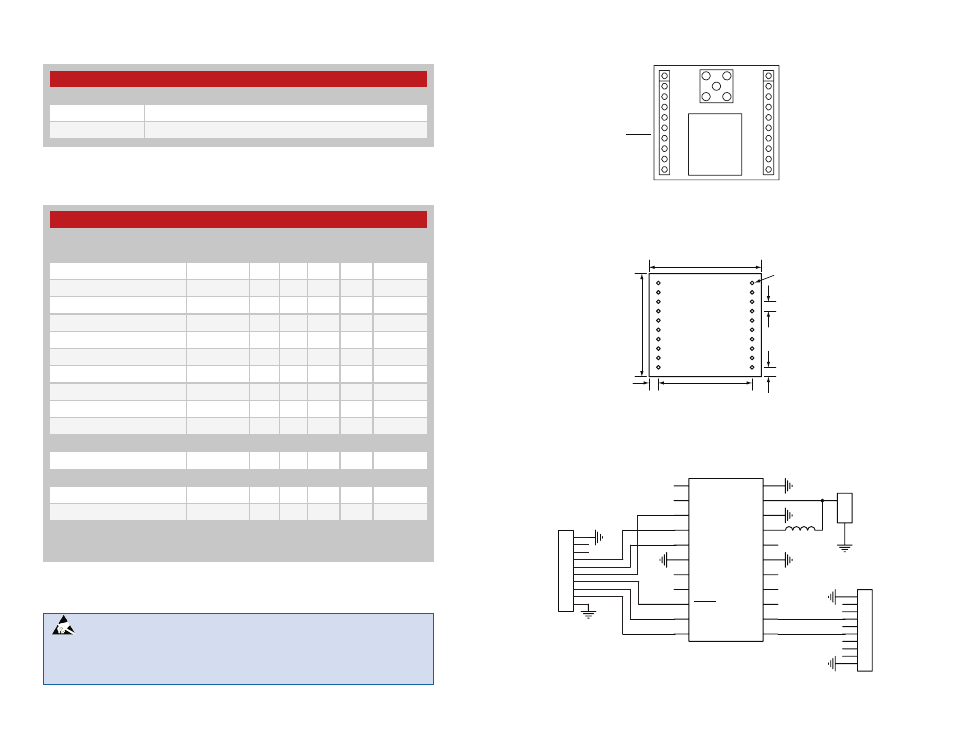
Pin Assignments
1.20”
(47.24)
0.10”
(2.54)
0.10”
(2.54)
0.10”
(2.54)
1.10”
(27.94)
1.00”
(25.40)
Ø0.04” x 10
(1.02)
GND
NC
NC
VCC
NC
VBACKUP
NC
NC
NC
GND
GND
NC
NC
TXM
RXM
1PPS
RESET
RFPWRUP
ON_OFF
GND
Figure 4: EVM-GPS-R4 Pin Assignments
PCB Layout
Figure 5: EVM-GPS-R4 PCB Layout Dimensions
Schematic
1
2
3
4
5
6
7
8
9
10
J1
GND
GND
1
2
3
4
5
6
7
8
9
10
J2
GND
GND
RF
GND
ANT1
CONREVSMA001
GND
GND
GND
GND
GND
NC
1
NC
2
1PPS
3
TXM
4
RXM
5
NC
6
NC
7
RESET
8
RRPWRUP
9
ON_OFF
10
VBACKUP
11
VIN
12
13
14
15
NC
16
VOUT
17
GND
18
RFIN
19
GND
20
GND
21
GND
22
U1
RXM-GPS-R4
L1
300ohm BEAD
NC
NC
NC
Figure 6: EVM-GPS-R4 Schematic