Typical applications, Xe1203f configuration registers – Linx Technologies TRM-xxx-DP1203 User Manual
Page 7
– –
– –
8
9
Figure 10 shows a typical read sequence from a configuration register.
Switching between Modes
The TRM-xxx-DP1203 is able to switch between two configurations by
using the 3-wire bus or by using the SWITCH line. Figure 11 shows the
switching sequence using the 3-wire bus to switch from Set #1 to Set #2.
In these examples, Set #1 is programmed to configure the module as a
transmitter and Set #2 is programmed to set the module as a receiver.
Figure 12 shows the switching sequence using the SWITCH line go change
from Set #1 to Set #2.
Mode
SWITCH Line (as input)
Set #1: Transmitter
Switching sequence using the SWITCH line
Switch_ext = 1 (Bit 3, Address 00010)
Set #2: Receiver
TX Line
RX Line
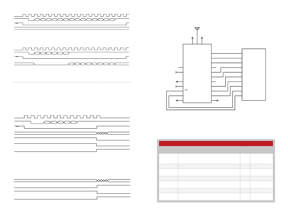
Typical Applications
The schematic in Figure 11 shows the TRM-xxx-DP1203 interfaced with a
microcontroller.
XE1203F Configuration Registers
Figure 14 shows the configuration registers in the XE1203F transceiver. For
more information on the registers please see the XE1203 Data Sheet.
SI
VCC
GND
GND
GND
GND
GND
VCC
GPIO
GPIO
GPIO
GPIO
GPIO
SCK
SO
SI
GPIO
GPIO
GND
3
AN
T
2
GND
1
VDDP
4
VDDA
5
GND
6
VDD
7
EN
8
SWITCH
9
GND
10
GND
11
SO
12
13
SCK
14
CLKOUT
15
DCLK
16
DATA
17
DATAIN
18
PATTERN
19
RX
20
TX
21
TRM-xxx-DP1203
µ
Figure 13: TRM-xxx-DP1203 Typical Application Schematic
SCK
SI
A4
A3
A2
A1
A0
D7 = 1
Mode
SWITCH Line (as output)
Switching sequence using the 3-wire bus
Switch_ext = 0 (Bit 3, Address 00010)
Set #1: Transmitter
Set #2: Receiver
EN
TX Line
RX Line
Figure 9: Write Sequence Into a Configuration Register
SCK
SI
EN
R/W
A4
A3
A2
A1
A0
D7
D6
D5
D4
D3
D2
D1
D0
SO
High Impedance
Figure 10: Read Sequence from a Configuration Register
SCK
SI
EN
R/W
A4
A3
A2
A1
A0
SO
D7
D6
D5
D4
D3
D2
D1
D0
High Impedance
High Impedance
Figure 11: Switching Sequence Using the 3-wire Bus
Figure 12: Switching Sequence Using the SWITCH Line
XE1203 Configuration Registers
Name
Description
Size
(bits)
Address
(Binary Format)
ConfigSwitch
1-bit data to switch between 2 sets of
user-predefined SWParam Configuration
Registers
1 x 1
00000
RTParam
Receiver and transmitter parameters
2 x 8
00001 - 00010
FSParam
LO, Bitrate, Deviation and other frequency
parameters
3 x 8
00011 - 00101
SWParam
2 sets of user-predefined configuration registers 6 x 8
00110 - 01011
DataOut
Status register which can be read through the
3-wire serial interface
2 x 8
01100 - 01101
ADParam
Additional parameters
5 x 8
01110 - 10010
Pattern
Reference pattern for the “pattern recognition”
feature
4 x 8
10011 - 10110
Figure 14: XE1203F Configuration Registers