Board layout guidelines, Power supply requirements, Schematic diagram – Linx Technologies EVM-915-250 User Manual
Page 6: Helpful application notes from linx
–
–
–
–
6
7
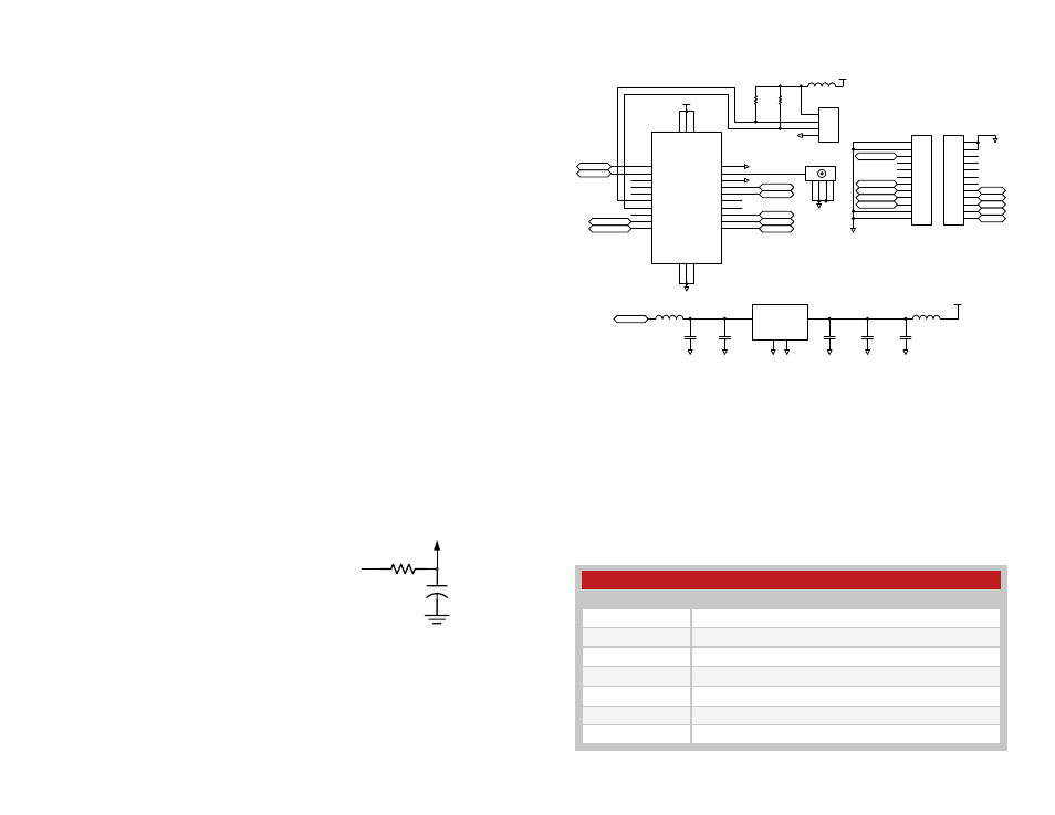
Schematic Diagram
1
2
3
4
5
6
7
8
9
10
11
12
JP2
GND
VIN
TXD
RXD
CMD
CTS
1
2
3
4
5
6
7
8
9
10
11
12
JP1
EX
RSSI
BE
GND
CMD_RSP
PR_PKT
IN
1
GND
2
GND
T
OUT
3
U1
GND
GND
VCC
47uF
C3
GND
4.7uF
C4
0.1uF
C5
GND
GND
4.7uF
C6
0.1uF
C7
GND
GND
L1
120NH
L3
120NH
VIN
J1
GND
CTS
TXD
RXD
PR_PKT
1
TXD
2
NC
3
NC
4
NC
5
RESET
6
C2D
7
NC
8
CMD_RSP
9
EX
10
GND
11
GND
12
GND
13
RSSI
14
CMD
15
BE
16
NC
17
NC
18
CTS
19
RXD
20
GND
21
ANT
22
GND
23
VCC
24
VCC
25
VCC
26
MOD1
VCC
GND
CMD_RSP
RSSI
BE
CMD
PR_PKT
EX
1
2
3
4
JP3
VCC
1K
R2
1K
R1
L2
120NH
GND
GND
GND
Board Layout Guidelines
The module’s design makes integration straightforward; however, it
is still critical to exercise care in PCB layout. Failure to observe good
layout techniques can result in a significant degradation of the module’s
performance. Grounding, filtering, decoupling, routing and PCB stack-up
are all important considerations for any RF design. Some basic design
guidelines are provided here.
The module should, as much as reasonably possible, be isolated from
other components on your PCB, especially high-frequency circuitry such as
crystal oscillators, switching power supplies, and high-speed bus lines.
When possible, separate RF and digital circuits into different PCB regions.
Make sure internal wiring is routed away from the module and antenna and
is secured to prevent displacement.
Bypass caps should be low ESR ceramic types and located directly
adjacent to the pin they are serving.
In some instances, a designer may wish to encapsulate or “pot” the
product. Since such compounds can considerably impact RF performance
and the ability to rework or service the product, it is the responsibility of the
designer to evaluate and qualify the impact and suitability of such materials.
Power Supply Requirements
The transceiver incorporates a precision
low-dropout regulator which allows operation
over a wide input voltage range. Despite this
regulator, it is still important to provide a supply
that is free of noise. Power supply noise can
significantly affect the module’s performance, so
providing a clean power supply for the module
should be a high priority during design.
A 10
Ω resistor in series with the supply followed by a 10μF tantalum
capacitor from V
cc
to ground helps in cases where the quality of supply
power is poor (Figure 7). This filter should be placed close to the module’s
supply lines. These values may need to be adjusted depending on the
noise present on the supply line.
Figure 8: 25 Series EVM Module Schematic
+
10
Ω
10
µF
Vcc IN
Vcc TO
MODULE
Figure 7: Supply Filter
Helpful Application Notes from Linx
It is not the intention of this manual to address in depth many of the issues
that should be considered to ensure that the modules function correctly
and deliver the maximum possible performance. As you proceed with your
design, you may wish to obtain one or more of the following application
notes which address in depth key areas of RF design and application of
Linx products. These application notes are available online at
www.linxtechnologies.com or by contacting Linx.
Helpful Application Note Titles
Note Number
Note Title
AN-00100
RF 101: Information for the RF Challenged
AN-00126
Considerations for Operation Within the 902–928MHz Band
AN-00130
Modulation Techniques for Low-Cost RF Data Links
AN-00140
The FCC Road: Part 15 from Concept to Approval
AN-00160
Considerations for Sending Data Over a Wireless Link
AN-00500
Antennas: Design, Application, Performance
AN-00501
Understanding Antenna Specifications and Operation
Figure 9: Helpful Application Notes