Yaskawa Drive Simulator User Manual
Page 9
TM.AFD.Simulator Page 9
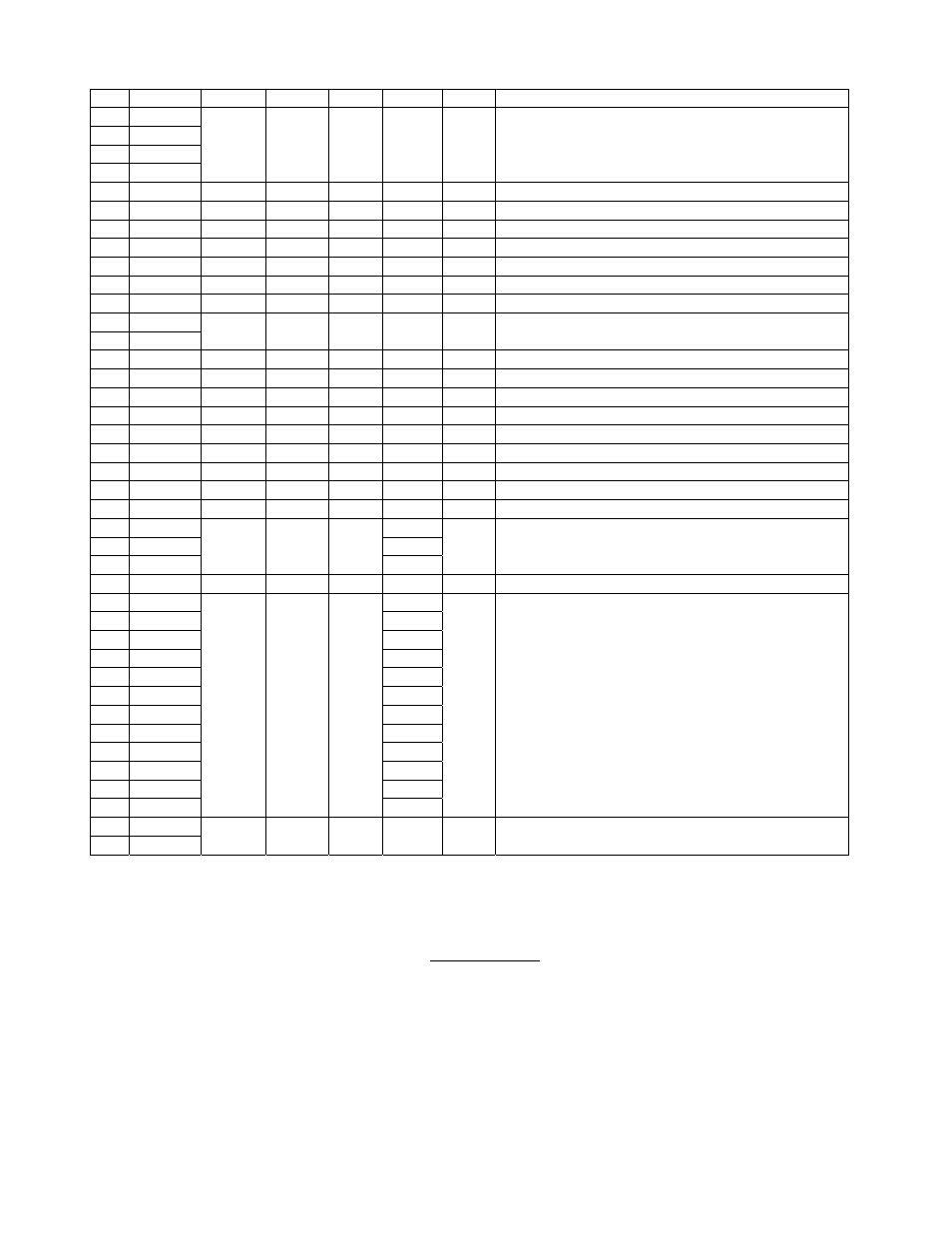
Pin Name I/O Type Level
Router
Logic
Description
1 US1
2 US2
3 US3
4 US4
Input Digital TTL S14/2 Low
The 4-Bit input code to assign the drive size, with
US1 being the LSB and US4, the MSB.
5
IP24V
Output
Supply
HTL
N/A
High
Unregulated 24VDC/200mA (25VDC) supply.
6
RDY
Output
Digital
TTL
None
Low
Goes Low when recycled control card is ready again.
7
FUL
Input
Digital
TTL
S18
Low
Should go low to induce a main DC Bus fuse failure.
8 RST Input
Digital
TTL
None
Low Should
go
low to recycle/reset control card power.
9
I_STAR
Output
Analog ±15V
None
N/A
Displays sum of the emulated three phase currents.
10 FAN Output
Digital
TTL None
High
Goes
high, should the blowers start working.
11 MCON Output Digital HTL None Low Goes
low when DC Bus Caps voltage is normal.
12 NWL
13 NW2L
Output Digital TTL None Low
Two PWM signals for lower half of one phase leg
directly from control card. See Note 4.
14 BTRA Input Digital TTL S14/3
High
Should go high when braking transistor is on.
15 BTRON Input Digital TTL S14/4
Low
Should go low to turn the braking transistor on.
16
MCOPL
Input
Digital
HTL
S16/1
High
Should go high to report soft starter relay is closed.
17
THM
Input
Analog
0-5V
S16/2
N/A
Lower the voltage, higher the temperature.
18 VDET Input Analog
-7.5V S16/3 N/A 0Æ-7.5V, more negative, higher DC bus voltage.
19
CUV
Input
Analog
3-5V
S16/4
N/A
Lower the voltage, less the control side voltage.
20
VCLL
Input
Digital
TTL
S13
Low
Should go low to report drive control low voltage.
21 VCHL Input Digital TTL S15 Low Should
go
low to report drive control high voltage.
22
VCFL
Input
Digital
TTL
S17
Low
Should go low to report power supply failure (SCL).
23 I_U
S22
24 I_V
S23
25 I_W
Input Analog ±15V
S24
N/A
They provide any arbitrary current waveform for the
control card under test, in any combination with or
without the internally emulated/controlled ones.
26 GND REF N/A 0V N/A N/A GROUND reference for all the I/O signals available.
27 DI-1
S1
28 DI-2
S2
29 DI-3
S3
30 DI-4
S4
31 DI-5
S5
32 DI-6
S6
33 DI-7
S7
34 DI-8
S8
35 DI-9
S9
36 DI-10
S10
37 DI-11
S11
38 DI-12
Input Digital
HTL
(24V)
S12
High
Provides the access to the user digital inputs of the
control card under test. DI-1 and DI-2 are reserved
for Run commands in all drives. DI-1..DI-7 inputs are
used in F7, E7 drives and DI-1..DI-8 for F7+ drives.
All 12 inputs are available to G7 drives. Should go
high to activate the inputs. To route each input to the
external port pins, the associated switch should be set
to EXT (external) position.
39 AIN1
40 AIN3
Input Analog ±10V S21 N/A
To feed the external reference value to the drive, VR1
and/or VR3 should be set to minimum (left) position.
Note 3: Although all the I/O pins in this port are protected against shorts or overloads but can still distort the normal
logical operations of the unit and/or control card under test circuitries, causing damage to them by improper
connections, high voltages, or shorting.
Note 4: These 2 PWM signals from the control card, NWL and NW2L should be probed/monitored very carefully
otherwise they can cause damage to the control card and/or unit motor emulator circuitry, in case of interference.