Isolated analog input option card ai-040 – Yaskawa AI-040 User Manual
Page 2
Yaskawa Electric America, Inc. – www.drives.com
IG.AFD.55, Page 2 of 4
Date: 10/07/05, Rev: 05-10
Isolated Analog Input Option Card
AI-040
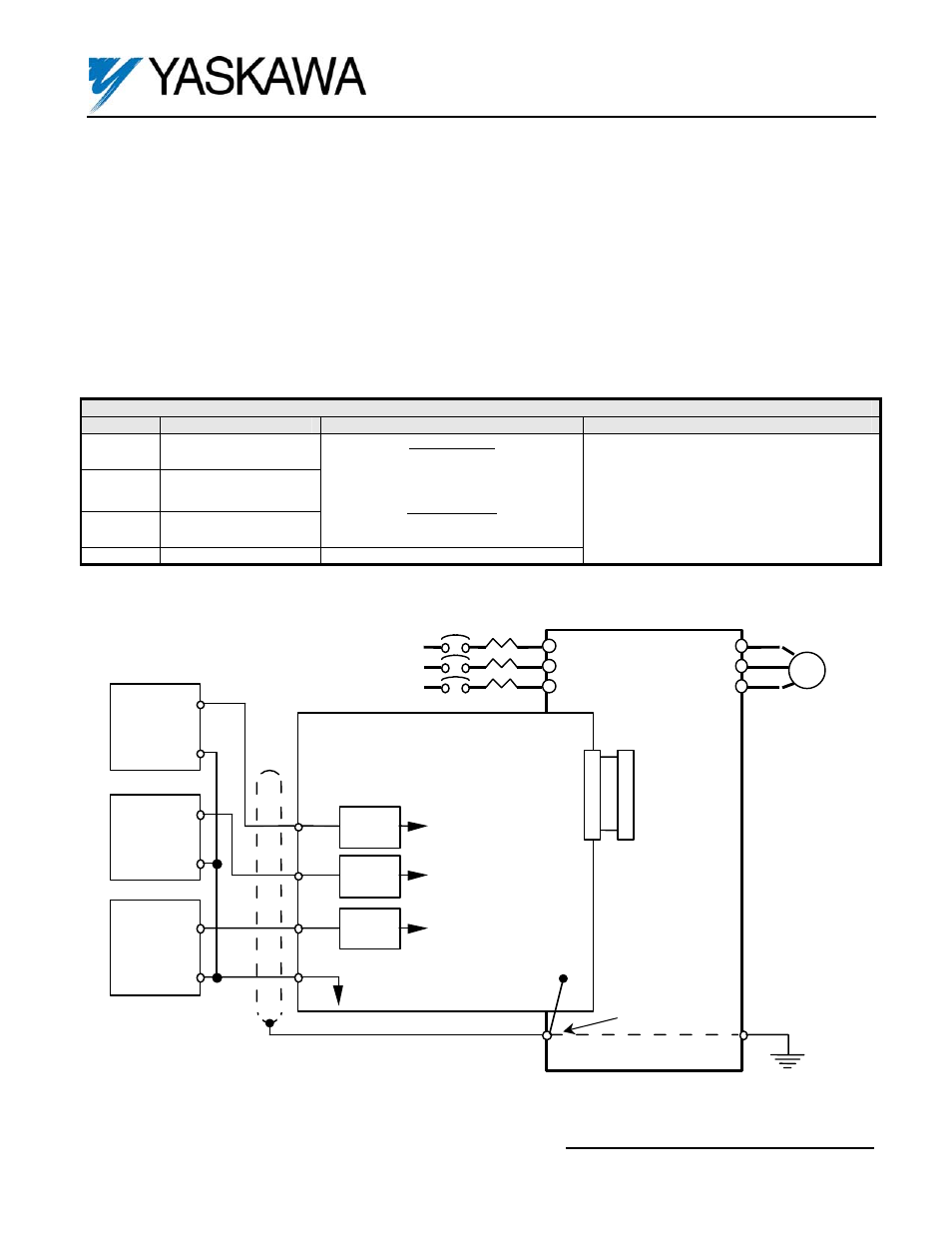
d) If any of the control signal input terminals (TC1-TC3) are NOT used, jumper them to 0V Terminal (TC4).
e) Route wires from the drive and connect to the peripheral device. Refer to the drive technical manual for further
information on use of shielded cable.
f)
Connect the option card ground wire (G1) to the drive’s ground terminal TB3 (12 for G5).
Important: Because the analog input is high-resolution, the voltage source accuracy of the analog input must be
considered. To ensure accuracy, use a high-precision power supply for the voltage source.
7. Adjustment. There are no adjustments to be made on the AI-040 option; however, the drive will have to be programmed
for the input requirement(s) of the remote device and the reversing or non-reversing requirement of the specific
application. Refer to Figures 4 and 5, and Table 3.
8. Reinstall and secure the drive’s front cover.
9. Place this instruction sheet with the drive’s technical manual.
Table 2. Terminal Functions of the AI-040
Terminal
Function
Signal Level
Notes
TC1
Analog
Voltage/Current Input
TC2
Analog
Voltage/Current Input
TC3
Analog
Voltage/Current Input
Voltage Input:
Input Voltage: 0 to +/-10V/0 to +/-100%
Input Impedance: 20Kohms
Current Input::
Input Current: 0 to 20mA/0 to 100%
Input Impedance: 500ohms
TC4 Signal
Common
0V
- Input Resolution:
Voltage: 1/8192 (13bit) + sign
Current: 1/6554
- Signal Linearity: +/-0.1%
- Terminal screws are metric size M3
2CN
Grounding Terminal
F7, G7: TB3
G5: 12
F7, G7,
GPD515/G5
AI-040 (AI-14B2) CARD
L1
L2
L3
T1
T2
T3
E
I M
Motor
MCCB
SHIELD
0V
High Accuracy
Voltage / Current
Devices
0V
2CN
14 BIT
A/D
14 BIT
A/D
14 BIT
A/D
See Figure 4
for
Block Diagram
0-±10VDC
or 0-20mA
0V
0V
TC1
TC2
TC3
TC4
0-±10VDC
or 0-20mA
0-±10VDC
or 0-20mA
G1
Figure 3. AI-040 Interconnection Diagram