Owner’s manual, Output stage block diagram – X-Treme Audio XTDT User Manual
Page 10
+
–
CH A input
+
–
CH B input
Vu Meter
Thermal Protect
Mute Bus
Thermal Protect
Mute Bus
1+
1-
2- 2+
CH A output
CH B output
LINK / BRIDGE
dip-switch
Mute Bus
Power supply
shutdown
HPF
(30 - 75 Hz)
Multiple
Gain
(26 ÷ 44 dB)
Limiter
Circuit
Error
amplifier
Modulator
Output
stage
driver
Half
bridge
power
stage
Fan
controller &
Thermal
monitor
Overcurrent
monitor
Clock
generator
and divider
DC
monitor
Output
low-pass
filter
HPF
(30 - 75 Hz)
Multiple
Gain
(26 ÷ 44 dB)
Limiter
Circuit
Error
amplifier
Modulator
Output
stage
driver
Half
bridge
power
stage
Fan
controller &
Thermal
monitor
Overcurrent
monitor
Clock
generator
and divider
DC
monitor
Output
low-pass
filter
-
+
-
+
1+
1-
2- 2+
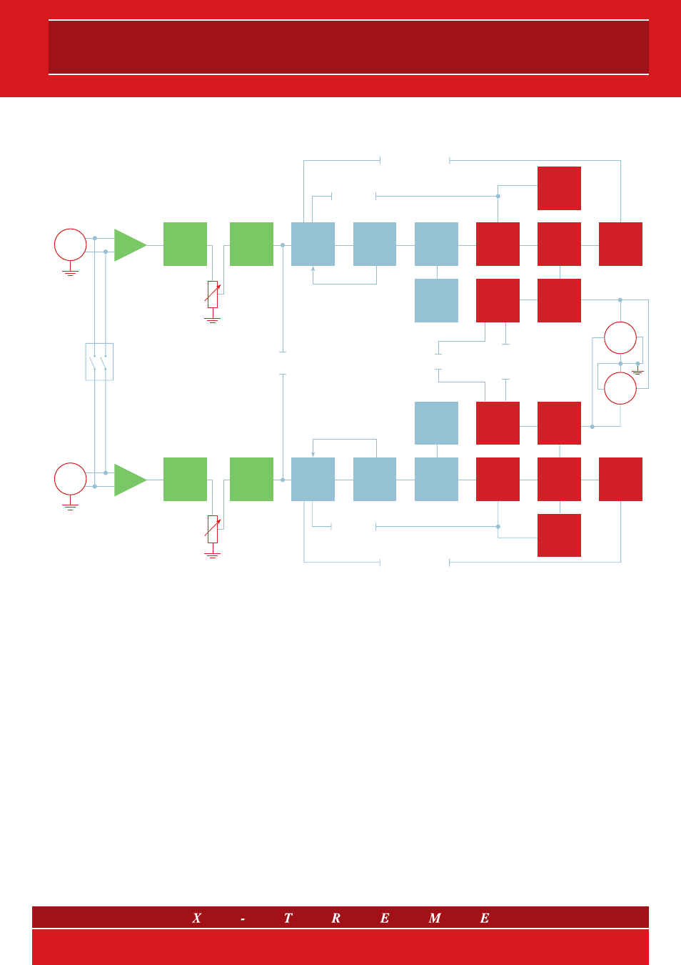
6. Output stage block diagram
fig. 8 Output stage block diagram - XTDT amplifiers
The figure above shows a block diagram displaying the output
stage of XTDT amplifiers (Class D).
XTDT digital amplifiers are provided with a
PWM-based techno-
logy (
Pulse Width Modulation) i.e. the input signal is converted
into a pulse sequence whose output values are higher than the
input ones. Over the time, the average pulse width values will be
directly proportional to the one-point amplitude of the input signal.
The output pulse frequency is typically 10 or more steps higher
than the one-point amplitude of the input signal. A low-pass filter
(LPF) removes the undesired signal components from the modu-
lation spectrum and yields an output signal corresponding to an
accurately amplified version of the input one.
10/14