Loops txport 400 rear panel, Switch s1, Dds net pinout – Verilink 400 (CG) Configuration/Installation Guide User Manual
Page 2: Dds s1 v.35, Net rs232, Sales and marketing, Returns/rma, Technical support
10
7
6
5
4
3
2
8
1
1
Data Out R
2
Data Out T
3 -6
Not Used
7
Data In T1
8
Data In R1
Ckt. V.35 RS-232
Signal Name - Function
(Note: all other pins are open)
DCE
101
A
1
Frame Ground - This circuit is used to terminate shields.
Gnd
102
B
7
Signal Ground - This circuit is used as the return reference for unbalanced signals.
Gnd
103
P/ S
2
Transmit Data - This input is used for synchronous TD from the DTE. It is transmitted on the DDS side.
In
104
R / T
3
Receive Data - This output is the data decoded from the incoming DDS receive data.
Out
105
C
4
Request To Send - This input is a control line from the DTE indicating data is to be transmitted. When RTS is On (space), the data transmitter,
the zero suppression circuitry, and the CTS are enabled. When RTS is Off, the transmitter sends idle code and the CTS is forced Off.
In
106
D
5
Clear To Send - This output is a DCE response, indicating that either RTS is On or S1 -8, position B, is forcing RTS ON. When S1 -7 is in
position B, RTS and RLSD must be On for CTS to be On.
Out
107
E
6
Data Set Ready - This output is On when the unit is not in a test mode (other than a V.54 test).
Out
109
F
8
Data Carrier Detect - This output is On when the correct data or zero suppression code is being received and DSR is On. It is Off when either
DSR is Off, the DDS receiver has lost sufficient signal to operate for at least one second, or the receiver has received OOS, OOF, idle, or loop
codes for about 20 U.I.
Out
113
U/ W
24
External Transmit Clock - This is the synchronous transmit clock input from the DTE. When both S1-3 and S1 -4 are in the B position, this
clock controls the frequency of the DDS transmit clock and clocks circuit 103 (TD). When either S1 -3 or S1-4 is in the A position, this input
has no effect on DDS operation.
In
114
Y/AA
15
Transmit Clock - This output is supplied by the DCE as an external DTE timing source. It is generated from the internal data clock or the far
end transmit data. Not available when S1 -3 and S1-4 are in the B position.
Out
115
V/ X
17
Receive Clock - This clock output is the timing for the RD and is always used to time the receive data. This clock is always derived from the
DDS receive data.
Out
142
K
25
Test Mode - This output is On when the unit is in the Test /Loop mode.
Out
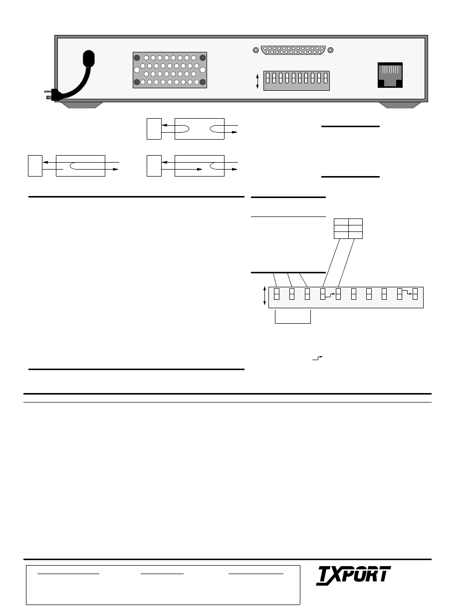
DDS NET Pinout
8
1
DDS
S1
V.35
115 VAC
A
B
13
1
14
25
NET
RS232
DTE
NET
Local Loopback
DTE
NET
Remote Channel Loop
(V.54) and Data Set Loop
DTE
NET
Channel Loop (Mandatory Loop)
Loops
TxPORT 400 Rear Panel
Rate
(kbps)
S1-1 S1- 2 S1- 3
RTS
to CTS
Delay
2.4
B
B
B
8 ms
4.8
A
B
B
4 ms
9.6
B
A
B
2 ms
19.2 A
A
B
1
ms
28 B
B
A
.8
ms
38.4 A
B
A
.5
ms
56 B
A
A
.4
ms
64 A
A
A
.3
ms
1-3 Channel Bitrate Select: These 3 positions select the channel bit rate (refer to the
table on the right). The RTS to CTS delays are multiplied by 2 when S1-10 is in the B
position.
4 Line Clock: This position selects either an internal clocking source or a loop timing
source from the received data.
5 Internal Clock: This position selects either the DSU external clock input or the
crystal oscillator as the clocking source. It is applicable only if S1-4 is in the B
position.
6 V.54 Loop Operation: This position enables or inhibits V.54 loop operation.
7 Data Polarity: This position determines whether data bits are inverted. In the A
position, marks equal pulses. In the B position, spaces equal pulses. Receipt of OOF,
OOS, idle, or loop codes forces the DSU data to all marks (A position) or spaces (B
position).
8 Circuit Assurance: On allows the status of CF (receive line signal detector) and CA
(request to send) to control the output CB (clear to send). If either CA or CF is Off
(position A), CB is Off. If CA and CF are On (position ‘B’), CB is On.
9 RTS/ CTS Control: In the B position, CTS is forced On regardless of the RTS input
status. In the A position, delays are determined by S1 -10.
10 RTS -> CTS Delay: In the A position, the RTS to CTS delay is as shown in the bit
rate table of the diagram. In the B position, the delays shown are multiplied by two.
6
5
4
3
1
7
9
8
2
Da
ta
Pola
rity
Cir
cui
t As
su
rance
R
T
S
/CT
S C
o
ntrol
Da
ta
Pola
rity
Cir
cuit As
su
rance
R
T
S
Nor
m
al Del
ay
Channel
Bit Rate
A
B
V
.54 L
oop
V
.5
4
L
oop
In
ternal Clock
L
in
e Clock
In
v
ert
ed
Nor
m
al
Of
f
On
En
ab
le
d
In
hibited
R
T
S
/CT
S Contr
o
l
R
T
S
Cont
rol
On
RT
S
->
C
T
S
D
el
ay
X 2
RT
S
->
C
T
S
D
el
ay
Nor
m
al
Note: The symbol ‘
’ indicates that the switch pointed to is not
functional unless the opposite end of the arrow is in the position shown.
For example, S1 - 5 is not functional unless S1 -4 is in the B position.
B
A
A
n/a
Master
Network (slave)
B
B
External
Switch S1
10
Sales and Marketing
800-285-2755
205-772-3770
Returns/RMA
800-926-0085, ext. 2282
205-772-3770, ext. 2282
Technical Support
800- 285-2755
205- 772-3770
9
V.35 and RS-232 Interface
127 Jetplex Circle
Madison, AL 35758
T
R
A
N
S
P
O
R
T
®