Loops – Verilink 300 (CG) Configuration/Installation Guide User Manual
Page 2
T
R
A
N
S
P
O
R
T
®
7
6
5
4
3
2
1
9
7
6
5
4
3
2
8
1
1 - 5 DSOs Assigned: These five positions select the bit rate and the number of DSOs assigned to the
channel (refer to the table below).
6
Rate Multiplier: Sets the multiplier for the input timing (refer to the table below). The unit oper-
ates at any data rate that is a multiple of 56 or 64 kb/s.
7
Channel Assignment: The Contiguous mode assigns the channels as a block beginning at DS0
channel 1. If ‘Alternate’ is selected, channel assignments are made with an idle channel following
each data channel.
8
Control Lines: ‘On’ permanently sets the CTS, DSR, and CD leads to ON. With ‘Follow’, the
DSR lead follows T1 sync, the CTS lead follows RTS, and the CD lead follows the density status of
the incoming T1 signal (Š 175 zeros = CD OFF). The TM line goes high when the unit is in a local
or remote test mode.
9
Data Invert: Determines whether the data bits are inverted.
6
5
4
3
1
7
9
8
2
56 kb/s
Conti
guous
Contr
o
l
D
ata
In
v
ert
64 k
b
/s
Alte
rn
at
e
C
o
ntrol
Data I
n
v
er
t
Follo
w
On
No
Ye
s
Switch S1
54016
ES
F
AM
I
T1
.4
0
3
D4
B8Z
S
5
4
3
2
1
6
7
B
A
A
A
B
A
Network clock (looped)
Internal clock (master)
CPE clock (external)
Timing
Source
Network
LBO
B
B
B
A
A
A
B
A
0
-22.5
-7.5
-15
Switch S2
DSO
S1 - 1
S1 - 2
S1 - 3
S1 - 4
S1 - 5
S1 - 6 (A)
S1 - 6 (B)
1
B B B B B 56
kb 64
kb
2
B A B B B 112
128
3
A A B B B 168
192
4
B B A B B 224
256
5
A B A B B 280
320
6
B A A B B 336
384
7
A A A B B 392
448
8
B B B A B 448
512
9
A B B A B 504
576
10
B A B A B 560
640
11
A A B A B 616
704
12
B B A A B 672
768
13
A B A A B 728
832
14
B A A A B 784
896
15
A A A A B 840
960
16
B B B B A 896
1024
17
A B B B A 952
1088
18
B A B B A 1008
1152
19
A A B B A 1064
1216
20
B B A B A 1120
1280
21
A B A B A 1176
1344
22
B A A B A 1232
1408
23
A A A B A 1288
1472
24
A A A A A 1344
1536
1
Data In (R1)
2
Data In (T1)
3/6
Not Used
4
Data Out (R)
5
Data Out (T)
7/8
Chassis Gnd
DTE
NET
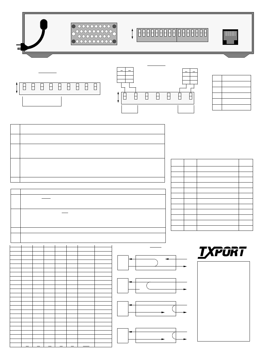
Local Loopback
DTE
NET
Remote Channel Loop (V.54)
DTE
NET
* Signal regeneration only
*
CSU Loop (FDL/PLB)
DTE
NET
* Signal, frame, and CRC regeneration
*
CSU Line Loop (Inband or FDL/LLB)
TxPORT 300 Rear Panel
Circuit Pin #
Signal Name
DCE
101
A
Frame Ground
Ground
102
B
Signal Ground
Ground
103
P/S
Transmit Data
In
104
R /T
Receive Data
Out
105
C
Request To Send
In
106
D
Clear To Send
Out
107
E
Data Set Ready
Out
109
F
Data Carrier Detect
Out
113
U /W
External Transmit Clock
In
114
Y/AA
Transmit Clock
Out
115
V/X
Receive Clock
Out
142
K
Test Mode
Out
V.35 Interface
NOTE: The ‘A’ position is the factory default for
all switch settings. If a particular user configura-
tion requires that a switch be placed in the ‘B’
direction, then mark this sheet for future reference.
DSOs Assigned
(see table at bottom)
Network Pinout
1 - 2 Timing Source: Selects the source of unit clocking (refer to the Switch S2 table).
3
ESF Mode: 54016 mode - unit responds only to 54016 CSU messages. T1.403 mode - unit
responds to ANSI loop/ unloop commands and generates a PRM every second, but will not respond
to 54016 messages.
4
Network Framing: In the ESF mode, the units can be configured for either the T1.403 or 54016
mode. In the 54016 mode, the unit responds to all 54016 messages. In the T1.403 mode, the unit
generates a PRM (performance report message) once every second and responds to T1.403 mes-
sages only.
5
Network Coding: Sets the network line code format.
6 - 7 Network LBO: Set the network signal level of data transmitted towards the T1 facility (refer to
table).
Switch S1 Description
Switch S2 Description
8
1
NET
S1
S2
V.35
93-130
VAC
A
B
A
B
A
B
127 Jetplex Circle
Madison, Alabama 35758
Sales and Marketing
800-926-0085
205-772-3770
RMA/ Returns
800- 926-0085, ext. 2282
Technical Support
800-285-2755
205-772-3770
B B Not Valid
Loops