4functional description, 1 block diagram – Sundance SMT166-FMC User Manual
Page 11
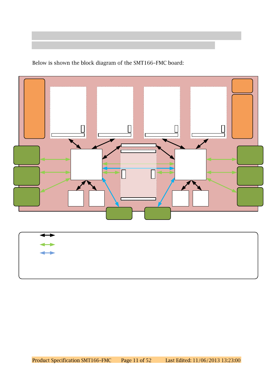
4
Functional Description
4.1
Block Diagram
SMT166
– SLB Carrier Board
SLB Bus
Rocket IOs
Parallel Bus
An SLB cable can be used to link the SLB on the Master module to the SLB on the SMT166 while using RSLs.
PCIe cable connectors can be used as a link to a host PC. 4 and 1-lane cables are available as well as Host Interface Board to communicate to a
PC.
FPGA_0
Virtex 6
LX130T-LX365T
SX315T-SX475T
PSU
Section
DDR3
Memory
Bank 2
FMC
Mezzanine 0
SLB
FMC
Mezzanine 1
SLB
FMC
Mezzanine 2
SLB
FMC
Mezzanine 3
SLB
FPGA_1
Virtex 6
LX130T-LX365T
SX315T-SX475T
DDR3
Memory
Bank 3
DDR3
Memory
Bank 0
DDR3
Memory
Bank 1
Fu
ll
SL
B
i
Fu
ll S
LB
j
Fu
ll
SL
B
l
Full S
LB
k
RSL x2
m
RSL x2
n
Ha
lf S
LB
n
Ha
lf S
LB
m
RSL x4
o
i
Channels x2
PCIe
Cable
x4
x4
l
Master
Module
SLB Connector
R
S
L
R
S
L
PCIe
Cable
x4
x4
j
PCIe
Cable
x1
x1
i
PCIe
Cable
x1
x1
k
USB+CPLD
+Flash
To configure
Virtex6
FPGAs and
access
Master
Module Flash
Clock
Synthesiser
Synchroniser
Top TIM Connector
Bottom TIM Connector
Dual
SATA3.0
x2
q
Dual
SATA3.0
x2
p
1Gigabit
Ethernet
1Gigabit
Ethernet
Figure 1 - SMT166-FMC Block Diagram.