IBASE MI970 User Manual
Page 16
INSTALLATIONS
12
MI970 User’s Manual
[
JP1: LPC debug Connector (Factory use only)
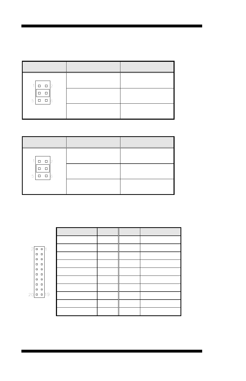
JP2: COM1 RS232 RI/+5V/+12V Power Setting
JP2
Setting
Function
Pin 1-2
Short/Closed
+12V
Pin 3-4
Short/Closed
RI
Pin 5-6
Short/Closed
+5V
JP3: COM2 RS232 RI/+5V/+12V Power Setting
JP3
Setting
Function
Pin 1-2
Short/Closed
+12V
Pin 3-4
Short/Closed
RI
Pin 5-6
Short/Closed
+5V
JP4, JP5: LVDS Connectors (1
st
channel, 2
nd
channel)
The LVDS connectors on board consist of the first channel (LVDS1) and
second channel (LVDS2).
Signal Name
Pin #
Pin #
Signal Name
TX0-
2
1
TX0+
Ground
4
3
Ground
TX1-
6
5
TX1+
5V/3.3V
8
7
Ground
TX3-
10
9
TX3+
TX2-
12
11
TX2+
Ground
14
13
Ground
TXC-
16
15
TXC+
5V/3.3V
18
17
ENABKL
+12V
20
19
+12V
This manual is related to the following products: