Chapter 2 - hardware installation, Board layout, Block diagram – DFI Q7-100 User Manual
Page 7: Q7 connector, Sd card, Spi glan usb 2.0 8x, Front audio spdif dvi vga
www.dfi .com
Chapter 2 Hardware Installation
7
Chapter 2
Chapter 2 - Hardware Installation
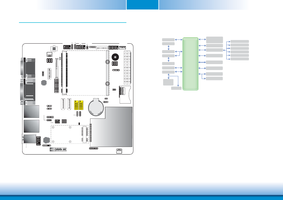
Board Layout
Block Diagram
COM 1
COM 2
VGA
DVI-I
DV
I-
I
p
ort
(DVI
-D
signal
only)
LAN 1
USB 1
USB 0
LAN 2
USB 2
USB 3
9 10
Front audio
2
1
Line-in/ Surround
Line-out
Mic-in/ Center+Subwoofer
Mini PCIe
S/PDIF
1
PCIe x1
Battery
1
CPU Fan
SPI Flash
BIOS
1
1
40
1
2
39
1
8
MXM
13
1
12
24
AT
X
p
o
w
er
1
7
1
7
SA
TA
1
SA
TA
0
USB 6-7
USB 4-5
2
9
10
9
10
1
2
1
1
1
1
1
1
1
1
1
1
1
1
1
1
2
6
5
1
2
6
5
1
1
2
12
11
Front panel
DIO
1
1
1
1
9
10
1
1
1
2
7
8
VGA/DVI
display
(JP8)
ExpressCard
SM Bus
SD/MMC
DIO Power
Select (J14)
I C
2
Chassis
Intrusion
LPC
SPI
USB 6-7 power
select (JP6)
USB 4-5
power
select (JP5)
LAN2/PCIe x1
Slot Function
Select (JP18)
MXM 5V power
select (JP2)
CAN-bus
Clear CMOS
(JP12)
System fan
USB 0-1 power
select (JP1)
LCD/ Inverter
power
LVDS LCD panel
CHRONTEL
CH7317B
Realtek
ALC886
LVDS Power
Select (JP14)
Battery Low
COM0
2
Super IO
Select (JP16)
USB 2-3 Power
Select (JP3)
USB Host/
Client Select
(JP7)
USB Client
Backlight control
level select (JP15)
BIOS Select
(J1)
Standby
Power Led
1
2
3
1
2
3
1
2
3
A
B
C
D
E
F
G
H
I
J
LAN2/PCIe x1 Slot
Function Select
(JP17)
COM0 RS232
Select (JP23)
Q7
Connector
ALC886
GLAN
(RTL8111DL)
SATA II 2x
Serial ATA
Interface
SD CARD
SDIO
Interface
Mini PCIe x1
PCIe x1
W83627DHG-P
PCIe x1
Interface
SDVO
Interface
CH7317
CH7318
LVDS
LVDS
Interface
SPI
GLAN
USB 2.0 8x
SPI
Interface
Front
Audio
SPDIF
DVI
VGA
USB
Interface
GPIO 8 Ports
H/W Monitor
CASE Open
CPU/SYS FAN
KB/MS
RS232 2x