Chapter 3 – DFI BT968 User Manual
Page 19
www.dfi .com
Chapter 3 Hardware Installation
19
Chapter 3
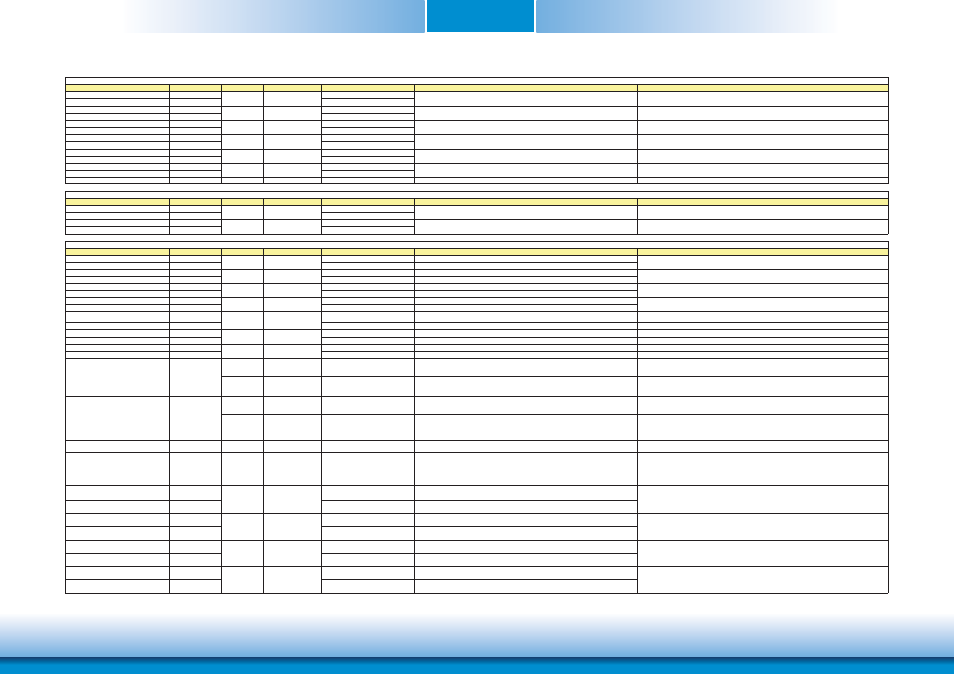
Signal
Pin#
Module Pin Type Pwr Rail /Tolerance
BT968
Carrier Board
Description
ȟ
ȟ
ȟ
ȟ
PEG Signals Descriptions
PEG_TX13+
D94
NA ==> (ALL PEG)
PEG_TX13-
D95
NA ==> (ALL PEG)
PEG_RX13+
C94
PEG_RX13-
C95
PEG_TX14+
D98
NA ==> (ALL PEG)
PEG_TX14-
D99
NA ==> (ALL PEG)
PEG_RX14+
C98
PEG_RX14-
C99
PEG_TX15+
D101
NA ==> (ALL PEG)
PEG_TX15-
D102
NA ==> (ALL PEG)
PEG_RX15+
C101
PEG_RX15-
C102
PEG_LANE_RV#
D54
I CMOS
3.3V / 3.3V
NA (No support)
NA (No support)
Signal
Pin#
Module Pin Type Pwr Rail /Tolerance
BT968
Carrier Board
Description
EXCD0_CPPE#
A49
EXCD1_CPPE#
B48
EXCD0_PERST#
A48
EXCD1_PERST#
B47
Signal
Pin#
Module Pin Type Pwr Rail /Tolerance
BT968
Carrier Board
Description
DDI1_PAIR0+/SDVO1_RED+
D26
Connect AC Coupling Capacitors 0.1uF to Device
DDI1_PAIR0-/SDVO1_RED-
D27
Connect AC Coupling Capacitors 0.1uF to Device
DDI1_PAIR1+/SDVO1_GRN+
D29
Connect AC Coupling Capacitors 0.1uF to Device
DDI1_PAIR1-/SDVO1_GRN-
D30
Connect AC Coupling Capacitors 0.1uF to Device
DDI1_PAIR2+/SDVO1_BLU+
D32
Connect AC Coupling Capacitors 0.1uF to Device
DDI1_PAIR2-/SDVO1_BLU-
D33
Connect AC Coupling Capacitors 0.1uF to Device
DDI1_PAIR3+/SDVO1_CK+
D36
Connect AC Coupling Capacitors 0.1uF to Device
DDI1_PAIR3-/SDVO1_CK-
D37
Connect AC Coupling Capacitors 0.1uF to Device
DDI1_PAIR4+/SDVO1_INT+
C25
NA (No support)
NA (No support)
DDI1_PAIR4-/SDVO1_INT-
C26
NA (No support)
NA (No support)
DDI1_PAIR5+/SDVO1_TVCLKIN+
C29
NA (No support)
NA (No support)
DDI1_PAIR5-/SDVO1_TVCLKIN-
C30
NA (No support)
NA (No support)
DDI1_PAIR6+/SDVO1_FLDSTALL+
C15
NA (No support)
NA (No support)
DDI1_PAIR6-/SDVO1_FLDSTALL-
C16
NA (No support)
NA (No support)
I/O PCIE
AC coupled on Module
PD 100K to GND
(S/W IC between Rpu/PCH)
Connect to DP AUX+
DP AUX+ function if DDI1_DDC_AUX_SEL is no connect
I/O OD CMOS
3.3V / 3.3V
PU 2.2K to 3.3V, PD 100K to GND
(S/W IC between Rpu/Rpd
resistor)
Connect to HDMI/DVI I2C CTRLCLK
HDMI/DVI I2C CTRLCLK if DDI1_DDC_AUX_SEL is pulled high
I/O PCIE
AC coupled on Module
PU 100K to 3.3V
(S/W IC between Rpu/PCH)
Connect to DP AUX-
DP AUX- function if DDI1_DDC_AUX_SEL is no connect
I/O OD CMOS
3.3V / 3.3V
PU 2.2K to 3.3V/PU 100K to 3.3V
(S/W IC between 2.2K/100K
resistor)
Connect to HDMI/DVI I2C CTRLDATA
HDMI/DVI I2C CTRLDATA if DDI1_DDC_AUX_SEL is pulled high
DDI1_HPD
C24
I CMOS
3.3V / 3.3V
PD 100K
PD 1M and Connect to device Hot Plug Detect
DDI Hot-Plug Detect
DDI1_DDC_AUX_SEL
D34
I CMOS
3.3V / 3.3V
PD 1M
PU 100K to 3.3V for DDC(HDMI/DVI)
Selects the function of DDI1_CTRLCLK_AUX+ and DDI1_CTRLDATA_AUX-.
DDI[n]_DDC_AUX_SEL shall be pulled to 3.3V on the Carrier with a 100K Ohm
resistor to configure the DDI[n]_AUX pair as the DDC channel.
Carrier DDI[n]_DDC_AUX_SEL should be connected to pin 13 of the DisplayPort
DDI2_PAIR0+
D39
Connect AC Coupling Capacitors 0.1uF to Device
(This Port is BIOS Option with On board LVDS (DP to LVDS))
DDI2_PAIR0-
D40
Connect AC Coupling Capacitors 0.1uF to Device
(This Port is BIOS Option with On board LVDS (DP to LVDS))
DDI2_PAIR1+
D42
Connect AC Coupling Capacitors 0.1uF to Device
(This Port is BIOS Option with On board LVDS (DP to LVDS))
DDI2_PAIR1-
D43
Connect AC Coupling Capacitors 0.1uF to Device
(This Port is BIOS Option with On board LVDS (DP to LVDS))
DDI2_PAIR2+
D46
Connect AC Coupling Capacitors 0.1uF to Device
(This Port is BIOS Option with On board LVDS (DP to LVDS))
DDI2_PAIR2-
D47
Connect AC Coupling Capacitors 0.1uF to Device
(This Port is BIOS Option with On board LVDS (DP to LVDS))
DDI2_PAIR3+
D49
Connect AC Coupling Capacitors 0.1uF to Device
(This Port is BIOS Option with On board LVDS (DP to LVDS))
DDI2_PAIR3-
D50
Connect AC Coupling Capacitors 0.1uF to Device
(This Port is BIOS Option with On board LVDS (DP to LVDS))
ȟ
ȟ
ȟ
ȟ
AC coupled off Module
O PCIE
O PCIE
AC coupled off Module
DDI 1 Pair 3 differential pairs/Serial Digital Video B clock output differential pair.
I PCIE
I PCIE
AC coupled off Module
AC coupled off Module
DDI Signals Descriptions
O PCIE
DDI 2 Pair 0 differential pairs
(This Port is BIOS Option with On board LVDS (DP to LVDS))
AC coupled off Module
DDI 1 Pair 0 differential pairs/Serial Digital Video B red output differential pair
I PCIE
O PCIE
AC coupled off Module
DDI 2 Pair 2 differential pairs
(This Port is BIOS Option with On board LVDS (DP to LVDS))
O PCIE
AC coupled off Module
DDI 2 Pair 1 differential pairs
(This Port is BIOS Option with On board LVDS (DP to LVDS))
DDI1_CTRLCLK_AUX+/SDVO1_CTRLCLK D15
DDI1_CTRLCLK_AUX-/SDVO1_CTRLDATA D16
AC coupled off Module
DDI 1 Pair 2 differential pairs/Serial Digital Video B blue output differential pair
O PCIE
AC coupled off Module
DDI 1 Pair 1 differential pairs/Serial Digital Video B green output differential pair
O PCIE
AC coupled off Module
O PCIE
AC coupled off Module
DDI 2 Pair 3 differential pairs
(This Port is BIOS Option with On board LVDS (DP to LVDS))
O CMOS
3.3V /3.3V
PCI ExpressCard: reset, active low, one per card
NA (No support)
ExpressCard Signals Descriptions
I CMOS
3.3V /3.3V
PCI ExpressCard: PCI Express capable card request, active low, one per
card
O PCIE
AC coupled on Module
NA (No support)
I PCIE
AC coupled off Module
NA (No support)
NA (No support)
NA (No support)
NA (No support)
NA (No support)
NA (No support)
NA (No support)
I PCIE
AC coupled off Module
NA (No support)
O PCIE
AC coupled on Module
NA (No support)
I PCIE
AC coupled off Module
O PCIE
AC coupled on Module
NA (No support)