Background – Dell JSM-6060LV User Manual
Page 4

J E O L J S M - 6 0 6 0 L V S C A N N I N G E L E C T R O N M I C R O S C O P E
3
Background
The scanning electron microscope (SEM) is one of the most versatile instruments for the
examination and analysis of the microstructural characteristics of solids. Although the SEM and
optical microscope share the same primary function – making microstructural features and objects
visible to the human eye – the scanning electron microscope offers some distinct advantages over
the optical microscope. The SEM uses electrons rather than visible light waves (200 – 750 nm
wavelength) for imaging, which allows for observation of relatively large sample features at low
magnifications or very fine details (high resolution) at high magnifications. The SEM also offers a
large depth of field that provides good focus over rough specimen surfaces. The large depth of
focus provides a three-dimensional appearance of the specimen in a SEM compared to the nearly
planar or two-dimensional imaging found in optical microscopes. In addition, many attachments
are available for scanning electron microscopes, including x-ray spectrometers for chemical
composition analysis, backscattered electron detectors for atomic number contrast, transmitted
electron detectors, hot and cold stages for microscopic observation of high or low temperature
phenomena, tensile testing stages for observation of deformation and fracture, and special stages
for analysis of semiconductor devices.
Disadvantages of the
scanning electron
microscope include
relatively high initial,
operational, and
maintenance costs, a high
vacuum operating
atmosphere that is
unsuitable for some
specimens, and difficulty in
preparing certain types of
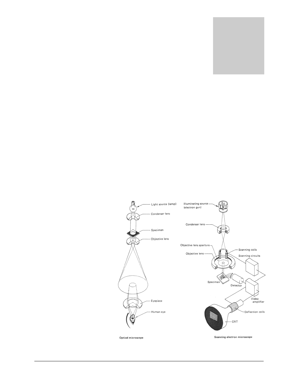
specimens. Figure 1
schematically illustrates
image formation in the
optical microscope and the
scanning electron
microscope.
2
Figure 1. Basic image formation in an optical microscope and a
scanning electron microscope.
