DeLorme GPS2058 User Manual
Page 11
5
5
4
4
3
3
2
2
1
1
D
D
C
C
B
B
A
A
GND
nSTDBYI
Wakeup
nRESET
Mod13_rsvd
Mod14_rsvd
Mod15_rsvd
PPS
GPIO2/I2C_CK
GPIO3/I2C_D
RF-GND
RF-IN
RF-GND
BOOTEN
JTCK
JTMS
USBDP
USBDN
JTDI
nJRST
U0RX
U1TX
U1RX
Mod36_rsvd
Mod35_rsvd
JTDO
U0TX
AIN0
AIN1
AIN2
AIN3
TRACKLED
GPIO1/SPIMOSI
GPIO0/SPIMISO
V18
GPIO3/SPI_SS/I2C_D
GPIO2/SPI_CK/I2C_CK
GPIO2/SPI_CK
GPIO3/SPI_SS
VADC
GPIO5/CANTX
GPIO4/CANRX
VCC Out
nSTDBYO
VCC In
Title
Size
Document Number
Rev
Date:
Sheet
of
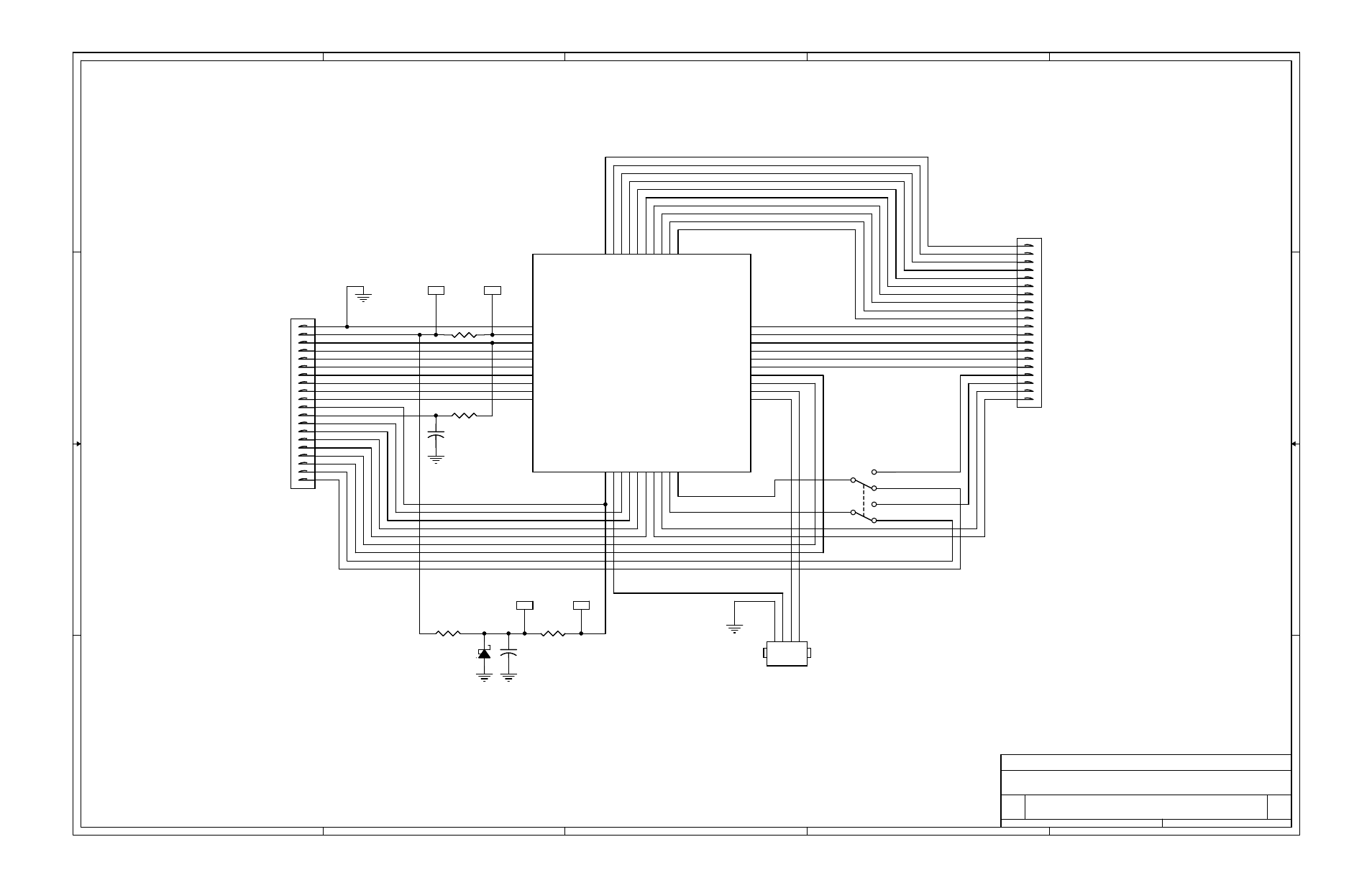
DeLORME_GPS2058_EVK_Adapter
C
GPS2058 Module Adapter PCB
B
1
1
Wednesday, April 23, 2008
Title
Size
Document Number
Rev
Date:
Sheet
of
DeLORME_GPS2058_EVK_Adapter
C
GPS2058 Module Adapter PCB
B
1
1
Wednesday, April 23, 2008
Title
Size
Document Number
Rev
Date:
Sheet
of
DeLORME_GPS2058_EVK_Adapter
C
GPS2058 Module Adapter PCB
B
1
1
Wednesday, April 23, 2008
GND, Pin 1
VCC IN, Pin 2
nSTDBYO, Pin 3
nSTDBYI, Pin 4
Wakeup, Pin 5
nRESET, Pin 6
AIN0, Pin 7
AIN1, Pin 8
AIN2, Pin 9
AIN3, Pin 10
VADC, Pin 11
VCC OUT, Pin 12
(Reserved), Pin 13
(Reserved), Pin 14
(Reserved), Pin 15
PPS, Pin 16
USBDP, Pin 17
USBDN, Pin 18
GPIO0/SPIMISO, Pin 21
GPIO1/SPIMOSI, Pin 22
GPIO2/SPI_CK, Pin 23
GPIO3/SPI_SS, Pin 24
JTCK, Pin 25
JTMS, Pin 26
JTDI, Pin 27
JTDO, Pin 28
nJTRST, Pin 29
U0RX, Pin 30
U1RX, Pin 32
U1TX, Pin 33
TRACKLED, Pin 34
U0TX, Pin 31
RF-GND, Pin 40
RF-IN, Pin 39
RF-GND, Pin 38
BOOTEN, Pin 37
(Reserved), Pin 36
(Reserved), Pin 35
MC/JP
J1 provides access to
V18 (Pin1,2) and CAN (Pin3,4)
SPI
I2C
GPIO3/I2C_D, Pin 20
GPIO2/I2C_CK, Pin 19
R4 10
R4 10
TP1
Test Point
TP1
Test Point
1
TP4
Test Point
TP4
Test Point
1
C1
10nF
C1
10nF
R1
10
R1
10
U1
GPS2058
U1
GPS2058
GND
1
VCC IN
2
nSTDBYO
3
nSTDBYI
4
WAKEUP
5
nRESET
6
AIN0
7
AIN1
8
AIN2
9
AIN3
10
U0TX/BOOT0
31
U1RX/BOOTRX
32
U1TX/BOOTTX
33
TRACKLED
34
Mod35_rsvd
35
Mod36_rsvd
36
BOOTEN
37
RF-GND1
38
RF-IN
39
RF-GND2
40
GPIO4/CANRX
21
GPIO5/CANTX
22
USBDP
23
USBDN
24
JTCK
25
JTMS
26
JTDI
27
JTDO
28
nJTRST
29
U0RX
30
VADC
11
V18
12
Mod13_rsvd
13
Mod14_rsvd
14
Mod15_rsvd
15
PPS
16
GPIO0/SPIMISO
17
GPIO1/SPIMOSI
18
GPIO2/SPI_CK/I2C_CK
19
GPIO3/SPI_SS/I2C_D
20
TP3
Test Point
TP3
Test Point
1
R3 0.1
R3 0.1
TP2
Test Point
TP2
Test Point
1
D1
MMBZ5222BLT1G
D1
MMBZ5222BLT1G
J11
PCB Contacts
J11
PCB Contacts
21
22
23
24
25
26
27
28
29
30
31
32
33
34
35
36
37
38
39
40
J1
Header_4pos
J1
Header_4pos
1 2 3 4
SW1
DPDT Slide
SW1
DPDT Slide
J10
PCB Contacts
J10
PCB Contacts
1
2
3
4
5
6
7
8
9
10
11
12
13
14
15
16
17
18
19
20
R2 0.1
R2 0.1
C2
0.1uF
C2
0.1uF