Intellijel Flip Flop User Manual
Intellijel, Flipflop manual

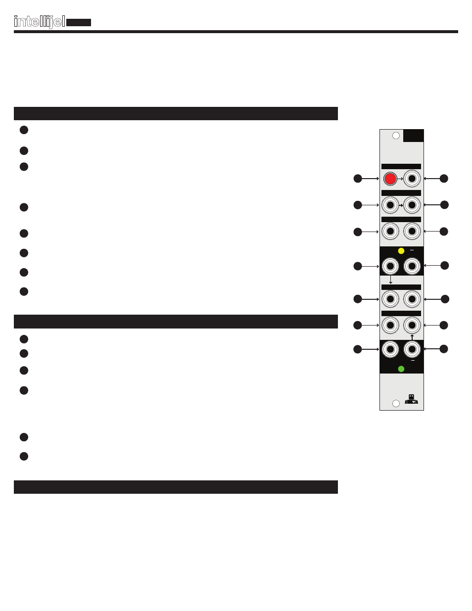
Manual Trigger: Creates a pulse that is normalled to the CLK input. Use this to manually create clock pulses as long as
there is nothing plugged into the CLK jack.
intellijel
designs
FlipFlop MANUAL
1
1
Clock Input: Clock input for the JK Flipflop. Feed a square/pulse 0-5V clock signal here.
2
Clock Input: Clock input for the D Flipflop. Feed a square/pulse 0-5V clock signal here.
9
3
4
5
6
7
8
9
10
11
13
2
J Input: J input for the JK Flipflop. Feed a square/pulse 0-5V clock signal here. This input is normalled to a positive
voltage refference (logic value of “HIGH”). This jacks is also normalled to the K input. In this configuration the JK
flipflop acts as a T flipflop (toggle) so that whenever it receives a clock pulse at the CLK input the outputs Q and
Qbar toggle between high and low. Ignoring the normalling, J is equivalent to a SET input except that it will only
make the flipflop output high when it has a positive pulse input at the same time as it gets a positive clock pulse.
3
D Input: D input for the D Flipflop. Feed a square/pulse 0-5V clock signal here. When nothing is patched here
the output of QBar is fed into this input. This causes the flipflop to toggle (act as a T flipflop) every time it receives a
clock pulse. When patching a pulse source here the output Q will follow whatever the value is at this input at the rising edge
of each clock pulse (i.e. if D input is low and the clock pulses, the output Q will go low, if D input is high and the clock pulses
then the output Q will go and stay high). Think of a D flipflop as a 1-bit memory cell where you can tell it what value to store
(0 or 1) either instantly using set/reset or in sync with a clock pulse.
12
12
14
Q
FLIPFLOP
Q
Q
Q
CLK
SET
RESET
D
J
K
SET
RESET
TRIG
CLK
K Input: K input for the JK Flipflop. Feed a square/pulse 0-5V clock signal here.
Ignoring the normalling (see above), K is equivalent to a RESET input except that it will only make the flipflop
output low when ithas a positive pulse input at the same time as it gets a positive clock pulse.
4
Set Input: Set input for the JK Flipflop. Feed a square/pulse 0-5V clock signal here.
A pulse here will trigger and instant high state at the output independent of any clock signal.
5
Set Input: Set input for the D Flipflop. Feed a square/pulse 0-5V clock signal here.
A pulse here will trigger and instant high state at the output independent of any clock signal.
10
Reset Input: Reset input for the JK Flipflop. Feed a square/pulse 0-5V clock signal here.
A pulse here will trigger and instant low state at the output independent of any clock signal.
6
Reset Input: Reset input for the D Flipflop. Feed a square/pulse 0-5V clock signal here.
A pulse here will trigger and instant low state at the output independent of any clock signal.
11
Q Output: Q Output of the flipflop. It’s state is indicated by the yellow led above it. This is a buffered logical output
than can be either high or low (0-8V). The output is normalled to the CLK input of the bottom D Flipflop.
7
Q Bar Output: The inverse of Q Output. It’s state is indicated as the opposite of the yellow led above it. This is a
buffered logical output than can be either high or low (0-8V).
8
Q Output: Q Output of the flipflop. It’s state is indicated by the yellow led above it. This is a buffered logical output
than can be either high or low (0-8V).
13
Q Bar Output: The inverse of Q Output. It’s state is indicated as the opposite of the yellow led above it. This is a
buffered logical output than can be either high or low (0-8V). The output is normalled to the D input.
The flipflop module comprises two indpendent CMOS flpflops. On the top half is a JK flipflop and on the bottom is a D flipflop. Through normalling,
both flipflops are configured to acts a toggle flipflops (each clock pulse causes there Q output to toggle) where the output of the JK flipflop is fed into
the clock input of the D flipflop. In this default configuration, the module is acting as a 2:1 and 4:1 clock divider. If you feed a clock source into the
JK CLK input the top output Q will be a 2:1 clock division. Since this 2:1 is feeding another flipflop below it (configured to toggle on clock pulses) then
the bottom Q output is a 4:1 division of the original clock signal. Since this is a discrete CMOS device you can feed extremely fast clock pulses. Try
feeding a square wave from a VCO and you will hear squarewaves that are 1 octave and 2 octaves below at the respective Q outputs.
For more info on Flipflops in general please visit : http://en.wikipedia.org/wiki/Flip-flop_%28electronics%29
INPUTS
Waveform: square or pulse waves ideally 0-5V (where 0V = logic low and 2V or greater is logic High)
max voltage: 10V
min voltage 0V
NOTE: unpredictable results with negtaive voltage
OUTPUTS
0-8V buffered
Max current draw: 15mA
14
D FlipFlop section
Technical Specs
JK FlipFlop section
