Chapter 3 – MSI A75A-G55 Manual User Manual
Page 49
BIOS Setup
MS-7695
Chapter 3
3-13
BIOS Setup
MS-7695
Chapter 3
tRC
The row cycle tme determnes the mnmum number of clock cycles a memory row
takes to complete a full cycle, from row actvaton up to the prechargng of the actve
row.
tWR
Mnmum tme nterval between end of wrte data burst and the start of a precharge
command. Allows sense amplfiers to restore data to cells.
tRRD
Specfies the actve-to-actve delay of dfferent banks.
tWTR
Mnmum tme nterval between the end of wrte data burst and the start of a column-
read command. It allows I/O gatng to overdrve sense amplfiers before read
command starts.
tRFC0/ 1
These settngs determne the tme RFC0/1 takes to read from and wrte to a memory
cell.
Advanced Channel 1/ 2 Tmng Configuraton
Press
for each channel.
tRWTT0/ tWRRD/ tWRWR/ tRDRD
These tems s used to set the memory tmngs for memory channel 1/ 2.
Bank Interleavng
Bank Interleavng s an mportant parameter for mprovng overclockng capablty of
memory. It allows system to access multple banks smultaneously.
NB Voltage/ DRAM Voltage/ SB Voltage
These tems are used to adjust the voltage of NB, memory and SB.
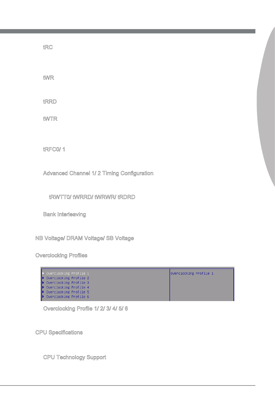
Overclockng Profiles
Press
Overclockng Profile 1/ 2/ 3/ 4/ 5/ 6
Press
the current settngs, and you can to load the settngs from the stored profile.
CPU Specficatons
Press
CPU.
CPU Technology Support
Press
technologes. Read only.
▶
▶
▶
▶
▶
▶
▶
▶
▶
▶
▶
▶
▶