A1323 – Allegro Multimedia A1321 User Manual
Page 3
recoverability after temperature cycling. Having the Hall element
and an amplifier on a single chip minimizes many problems normally
associated with low-level analog signals.
Output precision is obtained by internal gain and offset trim adjustments
made at end-of-line during the manufacturing process.
The A132X family is provided in a 3-pin single in-line package
(UA) and a 3-pin surface mount package (LH). Each package is
available in a lead (Pb) free version (suffix, –T) , with a 100% matte
tin plated leadframe.
Description (continued)
Ratiometric Linear Hall Effect Sensor ICs
for High-Temperature Operation
A1321, A1322,
and
A1323
2
Allegro MicroSystems, Inc.
115 Northeast Cutoff
Worcester, Massachusetts 01615-0036 U.S.A.
1.508.853.5000; www.allegromicro.com
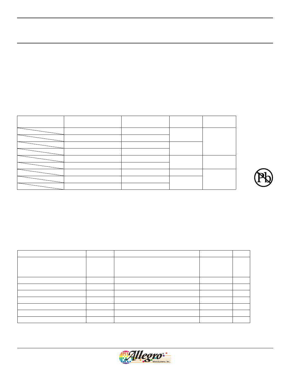
Selection Guide
Part Number
Packing
1
Mounting
Ambient, T
A
(ºC)
Sensitivity,
Typ. (mV/G)
A1321ELHLT-T
2
7-in. reel, 3000 pieces/reel
Surface Mount
–40 to 85
5.000
A1321EUA-T
3
Bulk, 500 pieces/bag
SIP through hole
A1321LLHLT-T
2
7-in. reel, 3000 pieces/reel
Surface Mount
–40 to 150
A1321LUA-T
3
Bulk, 500 pieces/bag
SIP through hole
A1322LLHLT-T
2
7-in. reel, 3000 pieces/reel
Surface Mount
–40 to 150
3.125
A1322LUA-T
3
Bulk, 500 pieces/bag
SIP through hole
A1323EUA-T
3
Bulk, 500 pieces/bag
SIP through hole
–40 to 85
2.500
A1323LLHLT-T
2
7-in. reel, 3000 pieces/reel
Surface Mount
–40 to 150
A1323LUA-T
3
Bulk, 500 pieces/bag
SIP through hole
1
Contact Allegro for additional packing options.
2
This variant is in production, however, it has been deemed Pre-End of Life. The product is approaching end of life. Within a minimum of 6 months,
the device will enter its final, Last Time Buy, order phase. Status change: January 31, 2011. Suggested replacements: for the A1321ELHLT-T and
the A1321LLHLT-T use the A1324LLHLX-T, for the A1322LLHLT-T use the A1325LLHLX-T, and for the A1323LLHLT-T use the A1326LLHLX-T.
3
Variant is in production but has been determined to be NOT FOR NEW DESIGN. This classification indicates that sale of the variant is currently
restricted to existing customer applications. The variant should not be purchased for new design applications because obsolescence in the near
future is probable. Samples are no longer available. Status change: January 31, 2011.
Absolute Maximum Ratings
Characteristic
Symbol
Notes
Rating
Units
Supply Voltage
V
CC
*
Additional current draw may be observed at
voltages above the minimum supply Zener
clamp voltage, V
Z(min)
, due to the Zener diode
turning on.
8
V
Output Voltage
V
OUT
8
V
Reverse Supply Voltage
V
RCC
–0.1
V
Reverse Output Voltage
V
ROUT
–0.1
V
Output Sink Current
I
OUT
10
mA
Operating Ambient Temperature
T
A
Range L
–40 to 150
ºC
Maximum Junction Temperature
T
J
(max)
165
ºC
Storage Temperature
T
stg
–65 to 170
ºC