2 the resistive touch pin-header (j101), Avr1909 – Atmel AVR1909 User Manual
Page 5
AVR1909
5
8297A-AVR-04/10
directly to the header. If it is desired to use PDI programming/debugging an adapter
or squid cable (included in the JTAGICE mkII kit) must be used. Please see Table 4-1
below for pin-out description.
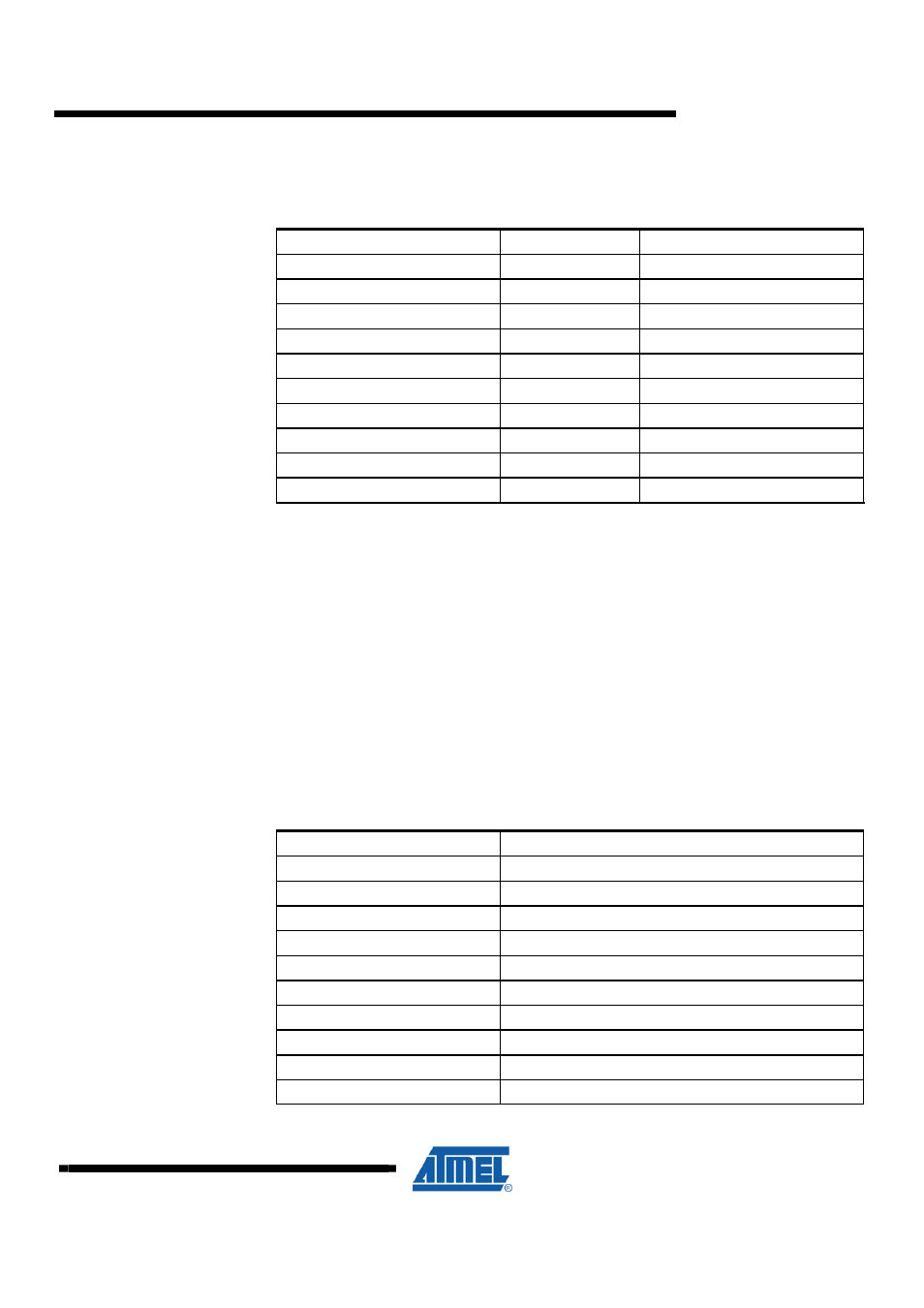
Table 4-1. Programming headers (J103/J104) – JTAG and PDI.
J103/J104 pin
JTAG
(1)
PDI
(2)
J103/J104-1 TCK
-
J103/J104-2 GND
GND
(3)
J103/J104-3 TDO
-
J103/J104-4 V3P3
V3P3
(3)
J103/J104-5 TMS
-
J103/J104-6 nSRST
PDI_CLK
J103/J104-7 V3P3
V3P3
(3)
J103/J104-8 -
PDI_DATA
J103/J104-9 TDI
-
J103/J104-10 GND
GND
(3)
Notes:
1. Standard pin-out for JTAGICE mkII and other Atmel programming tools.
2. Requires adapter or squid cable to connect a JTAGICE mkII (refer to AVR
Studio help).
3. It is only required to connect one V3P3/GND pin.
The AT90USB1287 can be programmed by connecting a programming tool, such as
a JTAGICE mkII, to the “JTAG USB” pin header (J200) on the Xplain board. Please
refer to AVR1907: Xplain Hardware User’s Guide for details.
4.2 The resistive touch pin-header (J101)
This connector connects the resistive touch interface to AVR XMEGA’s analog
PORTA that is available on the “XMEGA PORT A” pin header on the Xplain board
(J101). This allows the user to connect external signals to the ADC, DAC and Analog
Comparators on PORTA. Please see Table 4-2 below for pin-out description
Table 4-2. The resistive touch pin-header (J101) connections.
J101 pin
LCD resistive touch signals
J101-1 -
J101-2 -
J101-3 -
J101-4 -
J101-5
TFT_XL (X-direction, Left side)
J101-6
TFT_XR (X-direction, Right side)
J101-7
TFT_YD (Y-direction, Bottom [lower] side
J101-8
TFT_YU (Y-direction, Upper side)
J101-9 GND
J101-10 -