Agilent Technologies HFBR 5203 User Manual
Page 7
7
NO INTERNAL CONNECTION
NO INTERNAL CONNECTION
HFBR-520X
TOP VIEW
V
EE
RD
RD
SD
V
CC
V
CC
TD
TD
V
EE
1
2
3
4
5
6
7
8
9
C1
C2
L1
L2
R2
R3
R1
R4
C5
C3
C4
R9
R10
V
CC
FILTER
AT V
CC
PINS
TRANSCEIVER
R5
R7
R6
R8
C6
RD
RD
SD
V
CC
TD
TD
TERMINATION
AT PHY
DEVICE
INPUTS
NOTES:
THE SPLIT-LOAD TERMINATIONS FOR ECL SIGNALS NEED TO BE LOCATED AT THE INPUT
OF DEVICES RECEIVING THOSE ECL SIGNALS. RECOMMEND 4-LAYER PRINTED CIRCUIT
BOARD WITH 50 OHM MICROSTRIP SIGNAL PATHS BE USED.
TERMINATION
AT TRANSCEIVER
INPUTS
R1 = R4 = R6 = R8 = R10 = 130 OHMS.
R2 = R3 = R5 = R7 = R9 = 82 OHMS.
C1 = C2 = C3 = C5 = C6 = 0.1 µF.
C4 = 10 µF.
L1 = L2 = 1 µH COIL OR FERRITE INDUCTOR.
Rx
Rx
Tx
Tx
V
CC
V
CC
protect it from mechanical and
ESD damage during shipment or
storage.
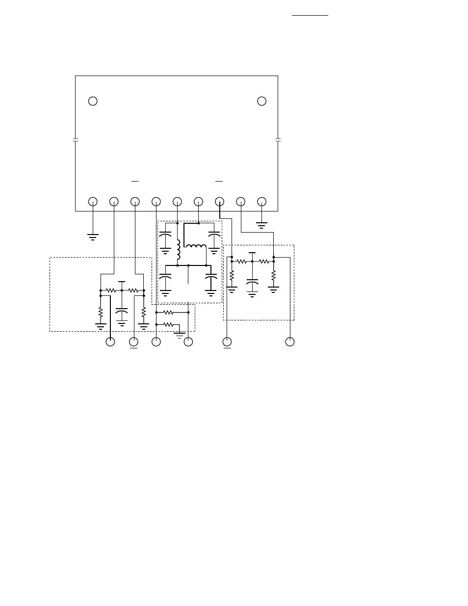
Board Layout - Decoupling
Circuit and Ground Planes
It is important to take care in the
layout of your circuit board to
achieve optimum performance
from these transceivers. Figure 7
provides a good example of a
schematic for a power supply
decoupling circuit that works well
with these parts. It is further
recommended that a contiguous
ground plane be provided in the
circuit board directly under the
transceiver to provide a low
inductance ground for signal
return current. This recommen-
dation is in keeping with good
high frequency board layout
practices.
Board Layout - Hole Pattern
The Agilent transceiver complies
with the circuit board “Common
Transceiver Footprint” hole
pattern defined in the original
multisource announcement which
defined the 1x9 package style.
This drawing is reproduced in
Figure 8 with the addition of ANSI
Y14.5M compliant dimensioning
to be used as a guide in the
mechanical layout of your circuit
board.
Figure 7. Recommended Decoupling and Termination Circuits.