Lvds interface, Table 3-7, Lvds interface pin/signal descriptions (j2) – Ampro Corporation AMPRO Single Board Computer MightyBoard 821 User Manual
Page 27
Chapter 3
Hardware
MightyBoard 821
Reference Manual
23
•
Supports Spread Spectrum Clocking; center and down spread support utilizing an external SSC clock
•
Supports panel up-scaling (to fit a smaller source image onto a specific native panel size) as well as
panning and centering CRT Interface
LVDS Interface
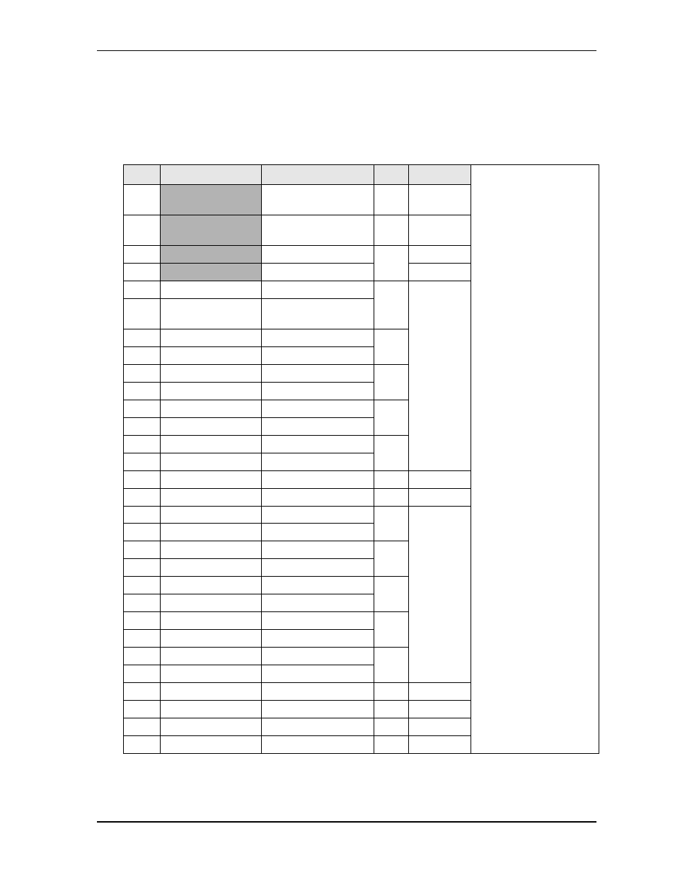
Note: The shaded area denotes power or ground.
Table 3-7. LVDS Interface Pin/Signal Descriptions (J2)
Pin #
Signal
Description
Line
Channel
NOTE
Pins 5-14
constitute 1st
channel
interface of
two channels,
or a single
channel
interface. Pins
17-26
constitute 2nd
channel
interface of
two channels.
1
+12V
JP5 = +5 or +12V
source
2
VCC_LCD
JP4 = +3.3 or +5V
source
3
GND
Ground
Gnd
4
GND
Ground
5
LVDSB_Clk+
Clock Positive Output
Clk
Channel 1
6
LVDSB_Clk-
Clock Negative
Output
7
NC
Not Connected
3
8
NC
Not Connected
9
LVDSB_Y2+
Data Positive Output
2
10
LVDSB_Y2-
Data Negative Output
11
LVDSB_Y1+
Data Positive Output
1
12
LVDSB_Y1-
Data Negative Output
13
LVDSB_Y0+
Data Positive Output
0
14
LVDSB_Y0-
Data Negative Output
15
LVD_BKLTCtl
Backlight Control
16
LCD_EN
LCD Enable
17
LVDSB_Clk+
Data Positive Output
Clk
Channel 2
18
LVDSB_Clk-
Data Negative Output
19
NC
Not Connected
3
20
NC
Not Connected
21
LVDSB_Y2+
Data Positive Output
2
22
LVDSB_Y2-
Data Negative Output
23
LVDSB_Y1+
Data Positive Output
1
24
LVDSB_Y1-
Data Negative Output
25
LVDSB_Y0+
Data Positive Output
0
26
LVDSB_Y0-
Data Negative Output
27
LVDS_DDCPClk
Clock
28
LVDS_DDCPData
Data
29
LVD_BKLEN
Backlight Enable
30
NC Not
connected