Gpio2x output control register – index 20h – AAEON TKS-G20-LN05 Rev.B User Manual
Page 50
E m b e d d e d C o n t r o l l e r
T K S - G 2 0 - L N 0 5 R e v . B
Appendix B DIO
B-2
B.1 DIO
The F75111 provides one serial access interface, I2C Bus, to
read/write internal registers. The address of Serial Bus is 0x6E
(0110_1110)
The related register for configuring DIO is list as follows:
Configuration and Control Register – Index 01h
Power-on default [7:0]=0000_1000b
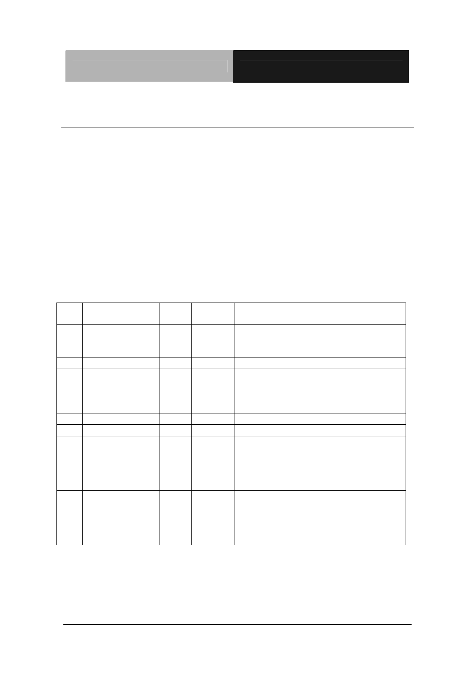
Bit Name
R/W
PWR Description
7
INIT
R/W
VSB3V
Software reset for all registers
including Test Mode registers. Users
use only.
6 Reserved
R/W
VSB3V
5
EN_WDT10
R/W
VSB3V
Enable Reset Out. If set to 1, enable
WDTOUT10# output. Default is
disable.
4 Reserved
R/W
VSB3V
3 Reserved
R/W
VSB3V
2 Reserved
R/W
VSB3V
1 SMART_POW
R_MANAGEM
ENT
R/W
VSB3V
Set this bit to 1 will enable auto power
down mode, when all function are idle
then 20ms the chip will auto power
down, it will wakeup when GPIO state
change or read write register
0 SOFT_POWR_
DOWN
R/W
VSB3V
Set this bit to 1 will power down all of
the analog block and stop internal
clock, write 0 to clear this bit or when
GPIO state change will auto clear this
bit to 0.
GPIO2x Output Control Register – Index 20h
Power-on default [7:0]=0000_1000b