Atmega16(l), Register summary (continued) – Rainbow Electronics atmega16p User Manual
Page 7
7
ATmega16(L)
2466BS–09/01
Notes:
1. When the OCDEN fuse is unprogrammed, the OSCCAL register is always accessed on this address. Refer to the debugger
specific documentation for details on how to use the OCDR register.
2. Refer to the USART description for details on how to access UBRRH and UCSRC.
3. For compatibility with future devices, reserved bits should be written to zero if accessed. Reserved I/O memory addresses
should never be written.
4. Some of the status flags are cleared by writing a logical one to them. Note that the CBI and SBI instructions will operate on
all bits in the I/O register, writing a one back into any flag read as set, thus clearing the flag. The CBI and SBI instructions
work with registers $00 to $1F only.
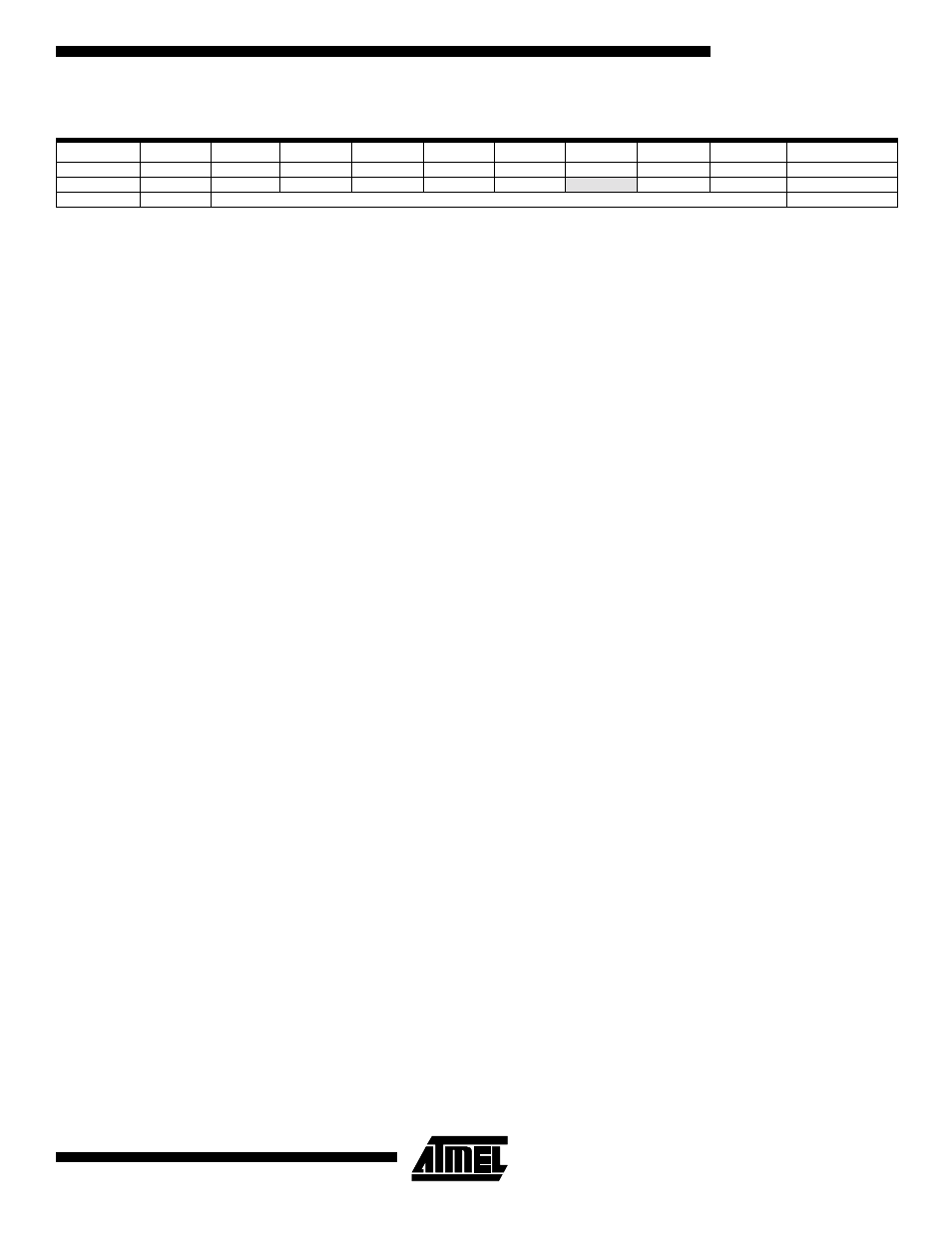
$02 ($22)
TWAR
TWA6
TWA5
TWA4
TWA3
TWA2
TWA1
TWA0
TWGCE
173
$01 ($21)
TWSR
TWS7
TWS6
TWS5
TWS4
TWS3
-
TWPS1
TWPS0
172
$00 ($20)
TWBR
2-wire Serial Interface Bit Rate Register
171
Register Summary (Continued)
Address
Name
Bit 7
Bit 6
Bit 5
Bit 4
Bit 3
Bit 2
Bit 1
Bit 0
Page