Chip information, Package information – Rainbow Electronics MAX684 User Manual
Page 9

MAX682/MAX683/MAX684
3.3V-Input to Regulated 5V-Output
Charge Pumps
_______________________________________________________________________________________
9
Power Dissipation
The power dissipated in the MAX682/MAX683/MAX684
depends on output current and is accurately described
by:
P
DISS
= I
OUT
(2V
IN
- V
OUT
)
P
DISS
must be less than that allowed by the package
rating. See the
Absolute Maximum Ratings
for 8-pin
µMAX (MAX683/MAX684) and SO (MAX682) power-
dissipation limits and deratings.
Layout Considerations
All capacitors should be soldered in close proximity to
the IC. Connect ground and power ground through a
short, low-impedance trace. If a high-value resistor is
driving the shutdown input and is picking up noise (i.e.,
frequency jitter at CXP and CXN), bypass SHDN to
GND with a small capacitor (0.01µF).
Paralleling Devices
The MAX682/MAX683/MAX684 can be paralleled to
yield higher load currents. The circuit of Figure 6 can
deliver 500mA at 5V. It uses two MAX682s in parallel.
The devices can share the output capacitors, but each
one requires its own transfer capacitor (C
X
) and input
capacitor. For best performance, the paralleled devices
should operate in the same mode (skip or constant fre-
quency).
Chip Information
TRANSISTOR COUNT: 659
SUBSTRATE CONNECTED TO GND
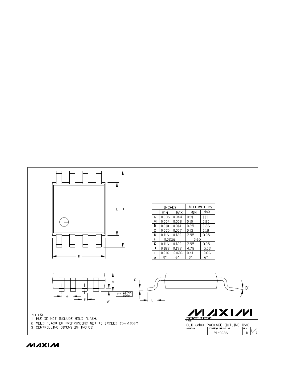
Package Information
8LUMAXD.EPS
