Rainbow Electronics MAX1681 User Manual
Page 2

V
MAX1680/MAX1681
125mA, Frequency-Selectable,
Switched-Capacitor Voltage Converters
2
_______________________________________________________________________________________
ABSOLUTE MAXIMUM RATINGS
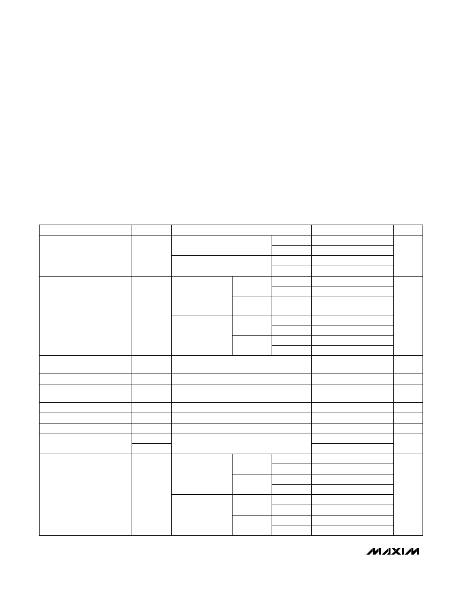
ELECTRICAL CHARACTERISTICS
(
Typical Operating Circuits
(inverter configuration), FSEL = LV = GND, V
IN
= 5V, C1 = C2 = 10µF (MAX1680), C1 = C2 = 2.2µF
(MAX1681),
T
A
= 0°C to +85°C
, unless otherwise noted. Typical values are at T
A
= +25°C.)
Stresses beyond those listed under “Absolute Maximum Ratings” may cause permanent damage to the device. These are stress ratings only, and functional
operation of the device at these or any other conditions beyond those indicated in the operational sections of the specifications is not implied. Exposure to
absolute maximum rating conditions for extended periods may affect device reliability.
IN ..............................................................................-0.3V to +6V
LV....................................................(V
OUT
- 0.3V) to (V
IN
+ 0.3V)
CAP+ ...........................................................-0.3V to (V
IN
+ 0.3V)
SHDN, FSEL ......................................(V
LV
- 0.3V) to (V
IN
+ 0.3V)
OUT, CAP- ..................................................................-6V to 0.3V
Continuous Output Current ..............................................135mA
Output Short-Circuit Duration to GND (Note 1) ...................1sec
Continuous Power Dissipation (T
A
= +70°C)
SO (derate 5.88mW/°C above +70°C) ..........................471mW
Operating Temperature Range ...........................-40°C to +85°C
Junction Temperature ......................................................+150°C
Storage Temperature Range .............................-65°C to +160°C
Lead Temperature (soldering, 10sec) .............................+300°C
I
LOAD
= 125mA
Inverter configuration,
R
L
= 1k
Ω
, LV = GND
LV = GND (Note 3)
FSEL = IN or LV
SHDN = IN
OUT = GND, SHDN = IN
CONDITIONS
375
500
625
750
1000
1250
94
125
156
187
250
313
4
V
IH
V
-3.75
-4.56
V
LOAD
Output Voltage Under Load
(Note 2)
V
3.0
5.5
2.0
5.5
V
1
V
IL
Shutdown, FSEL Thresholds
µA
-1
1
I
FSEL
Input Bias Current (FSEL)
Ω
3.5
10
R
OUT
Output Resistance (Note 2)
Ω
1
5
R
OUT(SHUT)
Output Resistance to Ground
in Shutdown
µA
1
I+
SHDN
Shutdown Current
µA
-1
1
I
SHDN
Input Bias Current (SHDN)
UNITS
MIN
TYP
MAX
SYMBOL
PARAMETER
Doubler configuration,
R
L
= 1k
Ω
, LV = OUT
4.0
5.5
V
IN
2.5
5.5
Input Voltage Range
MAX1680
5.4
mA
10.8
FSEL = IN
(125kHz)
FSEL = LV
(250kHz)
MAX1681
21.6
43.2
I+
FSEL = IN
(500kHz)
Supply Current
FSEL = LV
(1MHz)
Note 1:
Shorting OUT to IN may damage the device and should be avoided.
T
A
= +25°C
T
A
= +25°C
T
A
= +25°C
T
A
= +25°C
MAX1681
MAX1680
MAX1681
MAX1680
T
A
= +25°C
T
A
= +25°C
T
A
= +25°C
T
A
= +25°C
2.5
4.5
5
9
10
18
20
36
FSEL = LV
157
348
FSEL = IN
MAX1680
79
174
FSEL = LV
570
1490
kHz
FSEL = IN
MAX1681
f
OSC
Switching Frequency
285
745
