Step-down dc-dc converters, Layout, Inverter configuration – Rainbow Electronics MAX653 User Manual
Page 11: Two aa batteries to 5v, 3.3v, or 3v

capacitor, even when the switch is off. This will usually not
be a problem for a 5V output at room temperature, since
the diode’s reverse leakage current and the feedback
resistors’ current typically drain the excess. However, if
the diode leakage is very low (which can occur at low
temperatures and/or small output voltages), charge may
build up on the output capacitor, making V
OUT
rise above
its set point. If this happens, add a small load resistor
(typically 1M
Ω
) to the output to pull a few extra
microamps of current from the output capacitor.
Layout
Several of the external components in a MAX639/
MAX640/MAX653 circuit experience peak currents up
to 600mA. Wherever one of these components con-
nects to ground, there is a potential for ground bounce.
Ground bounce occurs when high currents flow
through the parasitic resistances of PC board traces.
What one component interprets as ground can differ
from the IC’s ground by several millivolts. This may
increase the MAX639/MAX640/MAX653’s output ripple,
since the error comparator (which is referenced to
ground) will generate extra switching pulses when they
are not needed. It is essential that the input filter capac-
itor’s ground lead, the MAX639/MAX640/MAX653’s
GND pin, the diode’s anode, and the output filter
capacitor’s ground lead are as close together as possi-
ble, preferably at the same point. Figure 5 shows a
suggested through-hole printed circuit layout that mini-
mizes ground bounce.
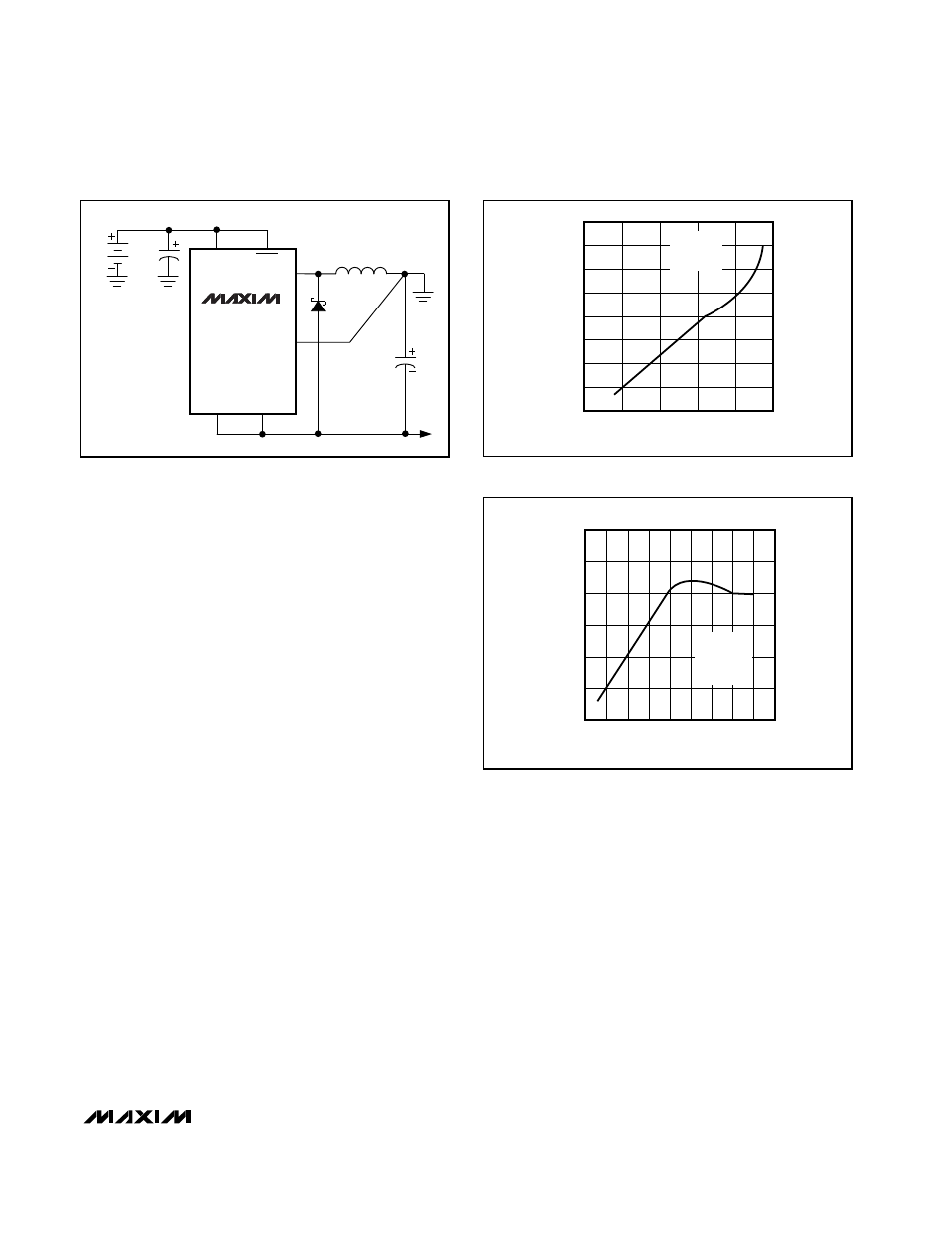
Inverter Configuration
Figure 6 shows the MAX639/MAX640/MAX653 in a
floating ground configuration. By tying what would nor-
mally be the output to the supply-voltage ground, the
IC’s GND pin is forced to a regulated -5V (MAX639),
-3.3V (MAX640), or -3V (MAX653). Avoid exceeding the
maximum differential voltage of 11.5V from V+ to V
OUT
.
Other negative voltages can be generated by placing a
voltage divider across C
OUT
and connecting the tap
point to VFB in the same manner as the normal step-
down configuration.
Two AA Batteries to 5V, 3.3V, or 3V
For battery-powered applications, where the signal
ground does not have to correspond to the power-supply
ground, the circuit in Figure 6 generates 5V (MAX639),
3.3V (MAX640), or 3V (MAX653) from a pair of AA batter-
ies. Connect the V
IN
ground point to your system’s input,
and connect the output to your system’s ground input.
This configuration has the added advantage of reduced
on resistance, since the IC’s internal power FET has V
IN
+
V
OUT
of gate drive (Figures 7 and 8).
MAX639/MAX640/MAX653
5V/3.3V/3V/Adjustable, High-Efficiency,
Low I
Q
, Step-Down DC-DC Converters
______________________________________________________________________________________
11
GND
MAX639
MAX640
MAX653
SHDN
LX
VOUT
-5V
-3.3V
OR -3V
4
V+
VFB
L = 100
µ
H
7
1
5
C
OUT
100
µ
F
V
IN
C
IN
100
µ
F
8
6
1N5817
Figure 6. Inverting Configuration
MAX639 FG02
MAXIMUM OUTPUT CURRENT (mA)
0
V+ (V)
T
A
= +25°C
L = 100
µ
H
MAX639
0
20
40
60
80
100
160
1
2
3
4
5
120
140
Figure 7. Maximum Current Capability of Figure 6 Circuit
MAX639 FG02
EFFICIENCY (%)
84.0
V+ (V)
T
A
= +25°C
V
OUT
= -5V
L = 470
µ
H
I
OUT
= 10mA
1.5
84.5
85.0
85.5
86.0
86.5
87.0
2.0 2.5 3.0 3.5 4.0 4.5 5.0
5.5 6.0
Figure 8. Efficiency of Figure 6 Circuit
