Pin description, Detailed description – Rainbow Electronics MAX889 User Manual
Page 5
MAX889
High-Frequency, Regulated,
200mA, Inverting Charge Pump
_______________________________________________________________________________________
5
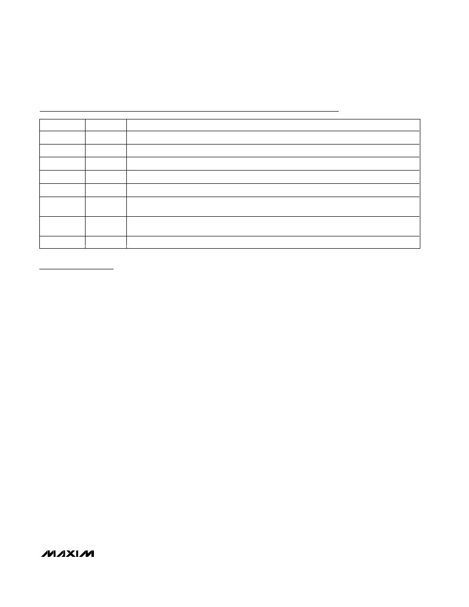
Pin Description
PIN
NAME
FUNCTION
1
IN
Power-Supply Positive Voltage Input
2
CAP+
Positive Terminal of Flying Capacitor
3
GND
Power Ground
4
CAP-
Negative Terminal of Flying Capacitor
5
OUT
Inverting Charge-Pump Output
6
SHDN
Shutdown Control Input. Drive SHDN low to shut down the MAX889. Connect SHDN to IN for
normal operation.
7
FB
Feedback Input. Connect FB to a resistor-divider from IN (or other positive reference voltage
source) to OUT for regulated output voltages. Connect to IN for free-run mode.
8
AGND
Analog Ground
Detailed Description
The MAX889 high-current regulated charge-pump DC-
DC inverter provides up to 200mA. It features the high-
est available output current while using small
capacitors (Table 1). The three versions available differ
in their switching frequencies (f
OSC
)—MAX889R/
MAX889S/MAX889T with f
OSC
= 500kHz/1MHz/2MHz,
respectively. Higher frequencies allow the use of small-
er components (Table 1). Even smaller capacitor values
than those listed in Table 1 are suitable when the
devices are loaded at less than their rated output cur-
rent. Designed specifically for compact applications, a
complete regulating circuit requires only three small
capacitors and two resistors, Figure 1. In addition, the
MAX889 includes soft-start, shutdown control, short-cir-
cuit, and thermal protection.
The oscillator, control circuitry, and four power MOSFET
switches are included on-chip. The charge pump runs
continuously at the operating frequency. During one-half
of the oscillator period, switches S1 and S2 close
(Figure 2), charging the transfer capacitor (C
FLY
) to the
input voltage (CAP- = GND, CAP+ = IN). During the
other half cycle, switches S3 and S4 close (Figure 3),
transferring the charge on C
FLY
to the output capacitor
(CAP+ = GND, CAP- = OUT).
Voltage Regulation
Voltage regulation is achieved by controlling the flying-
capacitor charging rate. The MAX889 controls the
charge on C
FLY
by modulating the gate drive to S1
(Figure 2) to supply the charge necessary to maintain
output regulation. When the output voltage droops,
C
FLY
charges higher due to increased gate drive. Since
the device switches continuously, the regulation
scheme minimizes output ripple, and the output noise
spectrum contains well-defined frequency components.
Feedback voltage is sensed with a resistor-divider
between an externally supplied positive reference or
the supply voltage and the negative inverted output.
The feedback loop servos FB to GND. The effective
output impedance in regulation is 0.05
Ω. The output
remains in regulation until dropout is reached. Dropout
depends on the output voltage setting and load current
(see Output Voltage vs. Load Current in Typical
Operating Characteristics).
Free-Run Mode
(Unregulated Voltage Inverter)
The MAX889 may be used in an unregulated voltage
inverter mode that does not require external feedback
resistors, minimizing board space. Connecting FB to IN
places the MAX889 in free-run mode. In this mode, the
charge pump operates to invert directly the input sup-
ply voltage (V
OUT
= -(V
IN
- I
OUT
x R
O
)). Output resis-
tance is typically 2
Ω and can be approximated by the
following equation:
R
O
≅ [1 / (f
OSC
x C
FLY
) ] + 2R
SW
+
4ESR
CFLY
+ ESR
COUT
The first term is the effective resistance of an ideal
switched-capacitor circuit (Figures 2 and 3), and R
SW
is the sum of the charge pump’s internal switch resis-
tances (typically 0.8
Ω at V
IN
= 5V). The last two terms
take into consideration the equivalent series resistance