Applications information, Table 1. input data byte (msb first) – Rainbow Electronics MAX1030 User Manual
Page 12
MAX1026/MAX1028/MAX1030
10-Bit 300ksps ADCs with FIFO,
Temp Sensor, Internal Reference
12
______________________________________________________________________________________
Applications Information
Register Descriptions
The MAX1026/MAX1028/MAX1030 communicate
between the internal registers and the external circuitry
through the SPI/QSPI-compatible serial interface. Table
1 details the registers and the bit names. Tables 2–7
show the various functions within the conversion regis-
ter, setup register, averaging register, reset register,
unipolar register, and bipolar register.
Conversion Time Calculations
The conversion time for each scan is based on a num-
ber of different factors: conversion time per sample,
samples per result, results per scan, if a temperature
measurement is requested, and if the external refer-
ence is in use.
Use the following formula to calculate the total conver-
sion time for an internally timed conversion in clock
modes 00 and 10 (see the Electrical Characteristics
section as applicable):
total conversion time = t
cnv
x n
avg
x n
result
+ t
TS
+ t
RP
where:
t
cnv
= t
acq
(max) + t
conv
(max)
n
avg
= samples per result (amount of averaging)
n
result
= number of FIFO results requested; determined
by number of channels being scanned or by NSCAN1,
NSCAN0
t
TS
= time required for temperature measurement; set
to zero if temp measurement is not requested
t
RP
= internal reference wake-up; set to zero if the inter-
nal reference is already powered up or if the external
reference is being used
In clock mode 01, the total conversion time depends on
how long CNVST is held low or high, including any time
required to turn on the internal reference. Conversion
time in externally clocked mode (CKSEL1, CKSEL0 = 11)
depends on the SCLK period and how long CS is held
high between each set of eight SCLK cycles.
Conversion Register
Select active analog input channels, scan modes, and
a single temperature measurement per scan by writing
to the conversion register. Table 2 details channel
selection, the four scan modes, and how to request a
temperature measurement. Request a scan by writing
to the conversion register when in clock mode 10 or 11,
or by applying a low pulse to the CNVST pin when in
clock mode 00 or 01.
A conversion is not performed if it is requested on a
channel that has been configured as CNVST or REF-.
Do not request conversions on channels 8–15 on the
MAX1026 and channels 12–15 on the MAX1028. Set
CHSEL3:CHSEL0 to the lower channel’s binary value. If
the last two channels are configured as a differential
pair and one of them has been reconfigured as CNVST
or REF-, the pair is ignored.
Select scan mode 00 or 01 to return one result per sin-
gle-ended channel and one result per differential pair
within the requested range, plus one temperature result if
selected. Select scan mode 10 to scan a single input
channel numerous times, depending on NSCAN1 and
NSCAN0 in the averaging register (Table 6). Select scan
mode 11 to return only one result from a single channel.
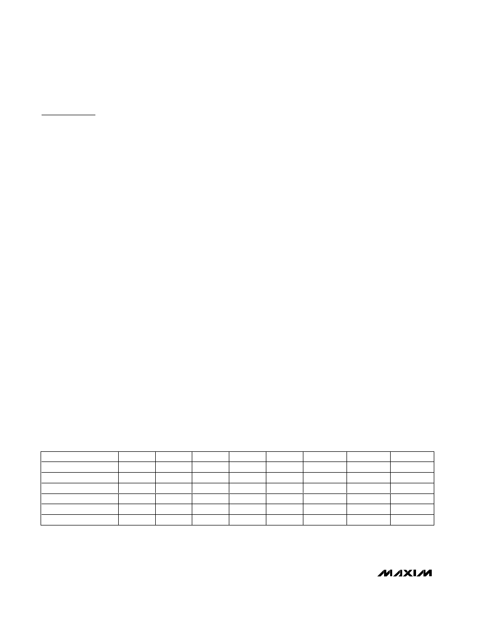
REGISTER NAME
BIT 7
BIT 6
BIT 5
BIT 4
BIT 3
BIT 2
BIT 1
BIT 0
Conversion
1
CHSEL3
CHSEL2
CHSEL1
CHSEL0
SCAN1
SCAN0
TEMP
Setup
0
1
CKSEL1
CKSEL0
REFSEL1
REFSEL0
DIFFSEL1
DIFFSEL0
Averaging
0
0
1
AVGON
NAVG1
NAVG0
NSCAN1
NSCAN0
Reset
0
0
0
1
RESET
X
X
X
Unipolar mode (setup)
UCH0/1
UCH2/3
UCH4/5
UCH6/7
UCH8/9*
UCH10/11*
UCH12/13**
UCH14/15**
Bipolar mode (setup)
BCH0/1
BCH1/2
BCH4/5
BCH6/7
BCH8/9*
BCH10/11*
BCH12/13**
BCH14/15**
Table 1. Input Data Byte (MSB First)
*Unipolar/bipolar channels 8–15 are only valid on the MAX1028 and MAX1030.
**Unipolar/bipolar channels 12–15 are only valid on the MAX1030.
X = Don’t care.