Reset, Low-input-voltage, 300ma ldo regulators with, Applications information – Rainbow Electronics MAX1976 User Manual
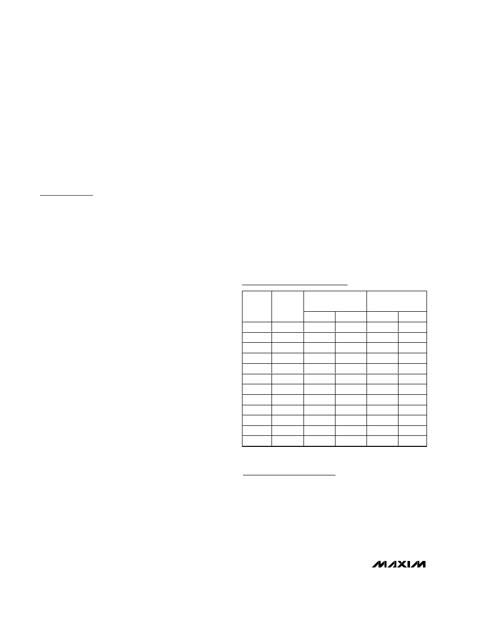
Page 8: Chip information, Selector guide

MAX1963/MAX1976
The MAX1963/MAX1976 deliver up to 300mA and oper-
ate with an input voltage up to +3.6V. However, when
using the 6-pin SOT23 version, high output currents
can only be sustained when the input-output differential
voltage is less than 2V, as shown in Figure 2.
The maximum allowed power dissipation for the 6-pin
TDFN is 1.951W at T
A
= +70°C. Figure 3 shows that the
maximum input-output differential voltage is not limited
by the TDFN package power rating.
Applications Information
Capacitor Selection and
Regulator Stability
Capacitors are required at the MAX1963/MAX1976
input and output for stable operation over the full tem-
perature range and with load currents up to 300mA.
Connect a 1µF ceramic capacitor between IN and GND
and a 4.7µF low-ESR ceramic capacitor between OUT
and GND. The input capacitor (C
IN
) lowers the source
impedance of the input supply. Use larger output
capacitors to reduce noise and improve load-transient
response, stability, and power-supply rejection.
The output capacitor’s equivalent series resistance
(ESR) affects stability and output noise. Use output
capacitors with an ESR of 30m
Ω or less to ensure sta-
bility and optimize transient response. Surface-mount
ceramic capacitors have very low ESR and are com-
monly available in values up to 10µF. Connect C
IN
and
C
OUT
as close to the MAX1963/MAX1976 as possible
to minimize the impact of PC board trace inductance.
Noise, PSRR, and Transient Response
The MAX1963/MAX1976 are designed to operate with
low dropout voltages and low quiescent currents in bat-
tery-powered systems while still maintaining good
noise, transient response, and AC rejection. See the
Typical Operating Characteristics for a plot of Power-
Supply Rejection Ratio (PSRR) versus Frequency.
When operating from noisy sources, improved supply-
noise rejection and transient response can be achieved
by increasing the values of the input and output bypass
capacitors and through passive filtering techniques.
The MAX1963/MAX1976 load-transient response (see
the Typical Operating Characteristics) shows two com-
ponents of the output response: a near-zero DC shift
from the output impedance due to the load-current
change, and the transient response. A typical transient
response for a step change in the load current from 20mA
to 200mA is 20mV. Increasing the output capacitor’s value
and decreasing the ESR attenuates the overshoot.
Input-Output (Dropout) Voltage
A regulator’s minimum input-output voltage difference
(dropout voltage) determines the lowest usable supply
voltage. In battery-powered systems, this determines the
useful end-of-life battery voltage. Because the
MAX1963/MAX1976 use a P-channel MOSFET pass tran-
sistor, the dropout voltage is a function of drain-to-source
on-resistance (R
DS(ON)
= 0.33
Ω) multiplied by the load
current (see the Typical Operating Characteristics).
V
DROPOUT
= V
IN
- V
OUT
= 0.33
Ω
✕
I
OUT
The MAX1963/MAX1976 ground current reduces to 70µA
in dropout.
Low-Input-Voltage, 300mA LDO Regulators
with
RESET
in SOT and TDFN
8
_______________________________________________________________________________________
Chip Information
TRANSISTOR COUNT: 2556
PROCESS: BiCMOS
MAX1963
TOP MARK
MAX1976
TOP MARK
V
OUT
(V)
SUFFIX
SOT
TDFN
SOT
TDFN
0.75
075
AABA
AFQ
AAAQ
AGA
0.85
085
—
—
AABP
AHD
1.00
100
—
—
AABL
AGC
1.10
110
—
—
AABM
AGD
1.20
120
AABE
AFU
AAAK
AGE
1.30
130
AABF
AFV
AABN
AGF
1.50
150
AABG
AFW
AAAL
AGG
1.60
160
—
—
AABO
AHC
1.80
180
AABH
AFX
AAAM
AGH
2.50
250
AABI
AFY
AAAN
AGI
2.85
285
—
—
AAAO
AGJ
3.00
300
AABJ
AFZ
AAAP
AGK
Selector Guide
