Pin description, Electrical characteristics (continued) – Rainbow Electronics MAX789 User Manual
Page 3
MAX787/MAX788/MAX789
5V/3.3V/3V 5A Step-Down, PWM,
Switch-Mode DC-DC Regulators
_______________________________________________________________________________________
3
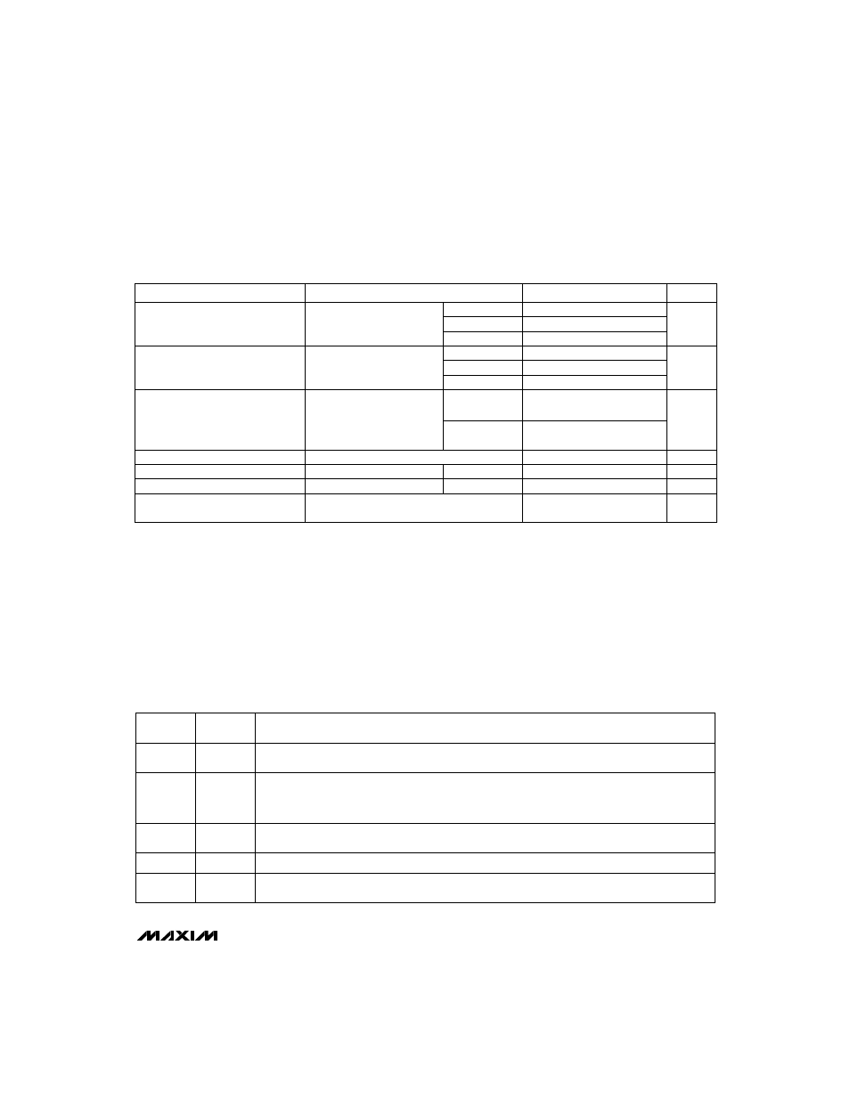
ELECTRICAL CHARACTERISTICS (continued)
(V
IN
= 25V, T
j
= T
MIN
to T
MAX
, unless otherwise noted.)
PARAMETER
MIN
TYP
MAX
UNITS
4.85
5.00
5.15
V
3.20
3.30
3.40
SENSE Voltage
V
C
= 2V
2.90
3.00
3.10
3.0
5.0
8.0
k
Ω
2.5
4.2
7.0
SENSE Pin Divider Resistance
T
j
= +25°C
2.2
3.8
6.5
CONDITIONS
MAX787
MAX788
MAX789
MAX787
MAX788
MAX789
T
j
= +25°C
±0.5
±2.0
%
Output Voltage Tolerance
V
OUT
(nominal) = 5V (MAX787),
3.3V (MAX788), or 3V (MAX789);
all conditions of input voltage,
output voltage, and load
current
T
j
= T
MIN
to
T
MAX
±1.0
±3.0
8V
≤
V
IN
≤
40V
0.005
0.020
%/V
Output Voltage Line Regulation
T
j
= +25°C
1.5
V
C
Voltage
T
j
= T
MIN
to T
MAX
-4
V
2.5
°C/W
Thermal Resistance Junction to Case
(Note 6)
mV/°C
V
C
Voltage Temperature Coefficient
0% duty cycle
0% duty cycle
Note 1:
Do not exceed switch-to-input voltage limitation.
Note 2:
For switch currents between 1A and 5A, maximum switch-on voltage can be calculated via linear interpolation.
Note 3:
By setting the SENSE pin to 5.5V, the V
C
pin is forced to its low clamp level and the switch duty cycle is forced to zero,
approximating the zero load condition.
Note 4:
For proper regulation, total voltage from V
IN
to GND must be
≥
8V after start-up.
Note 5:
To avoid extremely short switch-on times, the switch frequency is internally scaled down when V
SENSE
is less than 2.6V
(MAX787), 2.0V (MAX788), or 1.8V (MAX789). Switch-current limit is tested with V
SENSE
adjusted to give a 1µs minimum
switch-on time.
Note 6:
Guaranteed, not production tested.
______________________________________________________________Pin Description
V
IN
supplies power to the internal circuitry and also connects to the collector of the internal power
switch. V
IN
must be bypassed with a low-ESR capacitor, typically 200µF or 220µF.
Internal Power Switch Output. The
S
witch output can swing 35V below ground and is rated for 5A.
Ground requires a short, low-noise connection to ensure good load regulation. The internal reference
is referred to GND, so errors at this pin are multiplied by the error amplifier.
Error-Amplifier Output. A series RC network connected to this pin compensates the MAX787/MAX788/
MAX789. Output swing is limited to about 5.8V in the positive direction and -0.7V in the negative direc-
tion. V
C
can also synchronize the MAX787/MAX788/MAX789 to an external TTL clock in the 115kHz to
170kHz range. See MAX724/MAX726 data sheet.
SENSE Input is the internal error amplifier's input, and should be directly connected to V
OUT
. SENSE
also aids current limiting by reducing oscillator frequency when V
OUT
is low.
V
IN
V
SW
GND
V
C
SENSE
5
NAME
4
3
2
1
FUNCTION
PIN