Table 3. setup register – Rainbow Electronics MAX1231 User Manual
Page 14
MAX1227/MAX1229/MAX1231
12-Bit 300ksps ADCs with FIFO,
Temp Sensor, Internal Reference
14
______________________________________________________________________________________
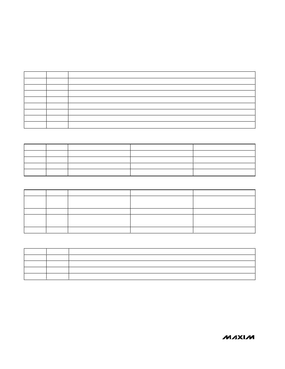
Table 3. Setup Register*
BIT NAME
BIT
FUNCTION
—
7 (MSB)
Set to zero to select setup register.
—
6
Set to 1 to select setup register.
CKSEL1
5
Clock mode and
CNVST configuration. Resets to 1 at power-up.
CKSEL0
4
Clock mode and
CNVST configuration.
REFSEL1
3
Reference mode configuration.
REFSEL0
2
Reference mode configuration.
DIFFSEL1
1
Unipolar/bipolar mode register configuration for differential mode.
DIFFSEL0
0 (LSB)
Unipolar/bipolar mode register configuration for differential mode.
CKSEL1
CKSEL0
CONVERSION CLOCK
ACQUISITION/SAMPLING
CNVST CONFIGURATION
0
0
Internal
Internally timed
CNVST
0
1
Internal
Externally timed through
CNVST
CNVST
1
0
Internal
Internally timed
AIN15/11/7
1
1
External (4.8MHz max)
Externally timed through SCLK
AIN15/11/7
REFSEL1
REFSEL0
VOLTAGE REFERENCE
AutoShutdown
REF- CONFIGURATION
0
0
Internal
Reference off after scan; need
wake-up delay.
AIN14/10/6
0
1
External single ended
Reference off; no wake-up delay.
AIN14/10/6
1
0
Internal
Reference always on; no wake-up
delay.
AIN14/10/6
1
1
External differential
Reference off; no wake-up delay.
REF-
DIFFSEL1
DIFFSEL0
FUNCTION
0
0
No data follows the setup byte. Unipolar mode and bipolar mode registers remain unchanged.
0
1
No data follows the setup byte. Unipolar mode and bipolar mode registers remain unchanged.
1
0
One byte of data follows the setup byte and is written to the unipolar mode register.
1
1
One byte of data follows the setup byte and is written to the bipolar mode register.
*See below for bit details.