Rainbow Electronics MAX1697 User Manual
Page 9
MAX1697
60mA, SOT23 Inverting Charge Pump
with Shutdown
_______________________________________________________________________________________
9
Surface-Mount
Tantalum
PRODUCTION
METHOD
714-969-2491
803-946-0690
PHONE
603-224-1961
603-224-1430
714-960-6492
803-626-3123
FAX
MANUFACTURER
AVX
Matsuo
Sprague
SERIES
TPS series
267 series
593D, 595D series
714-969-2491
803-946-0690
AVX
Matsuo
714-960-6492
803-626-3123
X7R
X7R
Surface-Mount
Ceramic
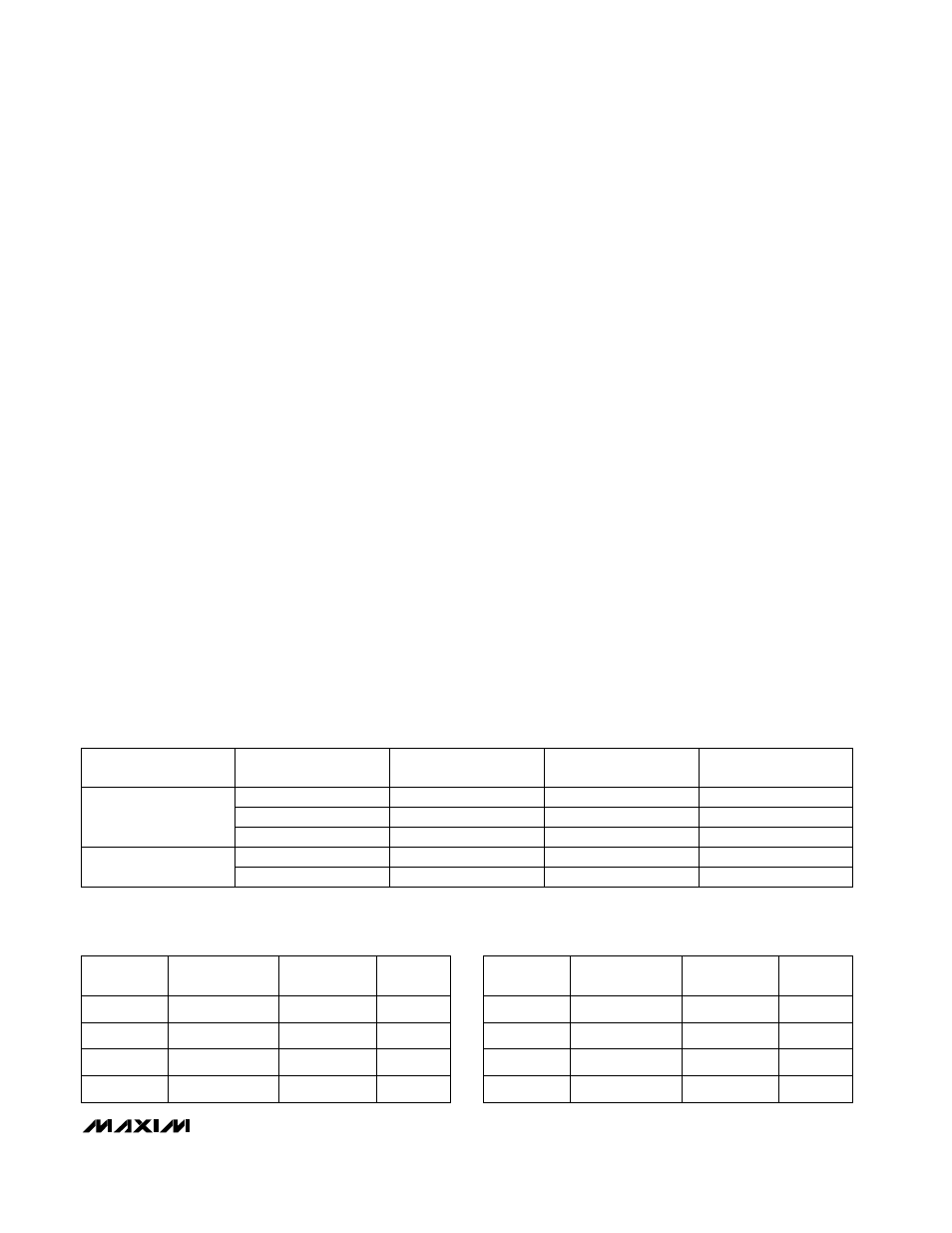
Table 2. Capacitor Selection to Minimize
Output Resistance
Table 3. Capacitor Selection to Minimize
Capacitor Size
Table 1. Low-ESR Capacitor Manufacturers
Voltage Inverter
The most common application for these devices is a
charge-pump voltage inverter (Figure 1). This applica-
tion requires only two external components—capacitors
C1 and C2—plus a bypass capacitor, if necessary.
Refer to the Capacitor Selection section for suggested
capacitor types.
Cascading Devices
Two devices can be cascaded to produce an even
larger negative voltage (Figure 4). The unloaded output
voltage is normally -2
✕
V
IN
, but this is reduced slightly
by the output resistance of the first device multiplied by
the quiescent current of the second. When cascading
more than two devices, the output resistance rises dra-
matically. For applications requiring larger negative
voltages, see the MAX865 and MAX868 data sheets.
Paralleling Devices
Paralleling multiple MAX1697s reduces the output resis-
tance. Each device requires its own pump capacitor
(C1), but the reservoir capacitor (C2) serves all devices
(Figure 5). Increase C2’s value by a factor of n, where n
is the number of parallel devices. Figure 5 shows the
equation for calculating output resistance.
Combined Doubler/Inverter
In the circuit of Figure 6, capacitors C1 and C2 form the
inverter, while C3 and C4 form the doubler. C1 and C3
are the pump capacitors; C2 and C4 are the reservoir
capacitors. Because both the inverter and doubler use
part of the charge-pump circuit, loading either output
causes both outputs to decline toward GND. Make sure
the sum of the currents drawn from the two outputs
does not exceed 60mA.
Heavy Load Connected to a
Positive Supply
Under heavy loads, where a higher supply is sourcing
current into OUT, the OUT supply must not be pulled
above ground. Applications that sink heavy current into
OUT require a Schottky diode (1N5817) between GND
and OUT, with the anode connected to OUT (Figure 7).
Layout and Grounding
Good layout is important, primarily for good noise per-
formance. To ensure good layout, mount all compo-
nents as close together as possible, keep traces short
to minimize parasitic inductance and capacitance, and
use a ground plane.
MAX1697R
MAX1697S
MAX1697T
MAX1697U
12
35
125
250
22
6.8
2.2
1
12
12
12
12
PART
FREQUENCY
(kHz)
CAPACITOR
(µF)
TYPICAL
R
OUT
(
Ω)
MAX1697R
MAX1697S
PART
MAX1697T
MAX1697U
FREQUENCY
(kHz)
CAPACITOR
(µF)
TYPICAL
R
OUT
(
Ω)
12
35
125
250
10
3.3
1
0.47
17
17
17
17