Max1124, Detailed description—theory of operation – Rainbow Electronics MAX1124 User Manual
Page 10

MAX1124
Detailed Description—Theory
of Operation
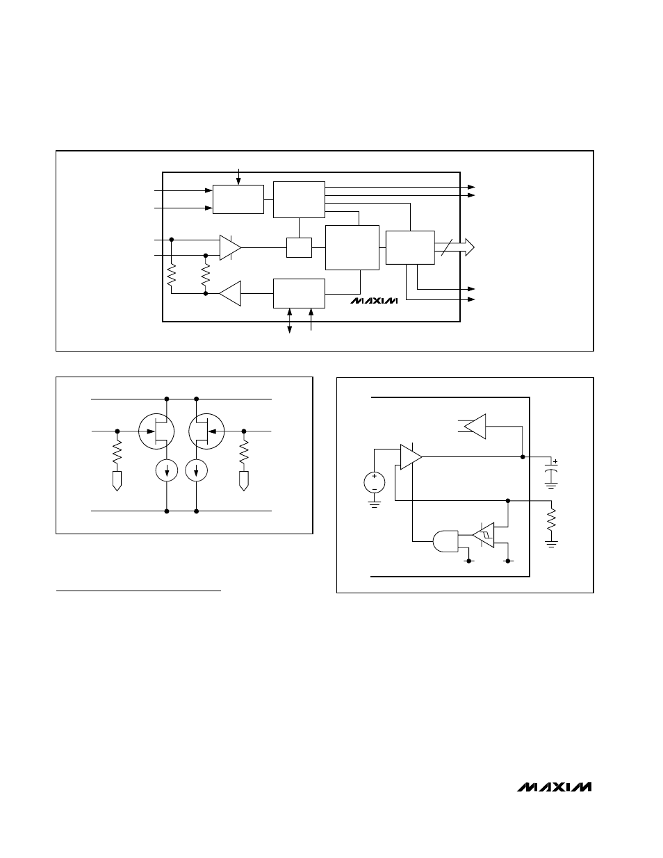
The MAX1124 uses a fully differential, pipelined archi-
tecture that allows for high-speed conversion, opti-
mized accuracy and linearity, while minimizing power
consumption and die size.
Both positive (INP) and negative/complementary analog
input terminals (INN) are centered around a common-
mode voltage of 1.4V, and accept a differential analog
input voltage swing of ±0.3125V each, resulting in a typi-
cal differential full-scale signal swing of 1.25V
P-P
.
INP and INN are buffered prior to entering each track-
and-hold (T/H) stage and are sampled when the differen-
tial sampling clock signal transitions high. A 2-bit ADC
following the first T/H stage then digitizes the signal, and
controls a 2-bit digital-to-analog converter (DAC).
Digitized and reference signals are then subtracted,
resulting in a fractional residue signal that is amplified
before it is passed on to the next stage through another
T/H amplifier. This process is repeated until the applied
input signal has successfully passed through all stages
of the 10-bit quantizer. Finally, the digital outputs of all
stages are combined and corrected for in the digital cor-
rection logic to generate the final output code. The result
is a 10-bit parallel digital output word in user-selectable
two’s complement or binary output formats with LVDS-
compatible output levels. See
Figure
1 for a more
detailed view of the MAX1124 architecture.
1.8V, 10-Bit, 250Msps Analog-to-Digital Converter
with LVDS Outputs for Wideband Applications
10
______________________________________________________________________________________
CLOCK-
DIVIDER
CONTROL
CLOCK
MANAGEMENT
T/H
10-BIT PIPELINE
QUANTIZER CORE
REFERENCE
LVDS
DATA PORT
10
COMMON-MODE
BUFFER
INPUT
BUFFER
CLKDIV
CLKP
CLKN
INP
INN
REFIO REFADJ
2.2kΩ
2.2kΩ
DCLKP
DCLKN
D0P/N–D9P/N
ORP
ORN
MAX1124
Figure 1. MAX1124 Block Diagram
AV
CC
AGND
INN
INP
TO COMMON-MODE INPUT
2.2kΩ
TO COMMON-MODE INPUT
2.2kΩ
Figure 2. Simplified Analog Input Architecture
REFERENCE
BUFFER
REFIO
REFADJ
AV
CC
AV
CC
/ 2
CONTROL LINE TO
DISABLE REFERENCE
BUFFER
ADC FULL-SCALE = REFT - REFB
G
1V
1kΩ
0.1µF
REFERENCE
SCALING
AMPLIFIER
REFT
REFB
Figure 3. Simplified Reference Architecture
