Design information – Rainbow Electronics MAX1745 User Manual
Page 10

MAX1744/MAX1745
High-Voltage, Step-Down DC-DC
Controller in µMAX
10
______________________________________________________________________________________
VL Linear Regulator
The MAX1744/MAX1745 contain a 5V low-side linear reg-
ulator (VL) that powers the internal circuit and can supply
up to 1mA to an external load. This allows the
MAX1744/MAX1745 to operate up to 36V input, while
maintaining low quiescent current and high switching fre-
quency. When the input voltage goes below 5.5V, this
regulator goes into dropout and the IN pin quiescent cur-
rent will rise. See the Typical Operating Characteristics.
Bypass VL with a 4.7µF or greater capacitor.
VH Linear Regulator
The MAX1744/MAX1745 contain a high-side linear reg-
ulator (VH) that regulates its output to 5V below IN (the
positive supply input voltage). This regulator limits the
external P-channel MOSFET gate swing (EXT), allowing
high input voltage operation without exceeding the
MOSFET gate-source breakdown. Bypass VH with a
4.7µF or greater capacitor between IN and VH.
Quiescent Current
The devices’ typical quiescent current is 90µA.
However, actual applications draw additional current to
supply MOSFET switching currents, OUT pin current,
external feedback resistors (if used), and both the diode
and capacitor leakage currents. For example, in the cir-
cuit of Figure 1, with IN at 30V and V
OUT
at 5V, typical
no-load supply current for the entire circuit is 100µA.
Shutdown Mode
When SHDN is low, the device enters shutdown mode. In
this mode, the internal circuitry is turned off. EXT is
pulled to IN, turning off the external MOSFET. The shut-
down supply current drops to less than 10µA. SHDN is a
logic-level input. Connect SHDN to IN for normal opera-
tion.
Reference
The 1.25V reference is suitable for driving small external
loads. It has a guaranteed 10mV maximum load regula-
tion while sourcing load currents up to 100µA. The refer-
ence is turned off during shutdown. Bypass the
reference with 0.1µF for normal operation. Place the
bypass capacitor within 0.2in (5mm) of REF, with a direct
trace to GND.
Design Information
Setting the Output Voltage
The MAX1744’s output voltage can be selected to 3.3V
or 5V under logic control by using the 3/5 pin. Connect
the 3/5 pin to GND to ensure a 3.3V output, or connect
the 3/5 pin to V
L
to ensure a 5V output.
The MAX1745’s output voltage is set using two resis-
tors, R2 and R3 (Figure 5), which form a voltage-divider
between the output and FB. R2 is given by:
R2 = R3 x
V
V
OUT
REF
−
1
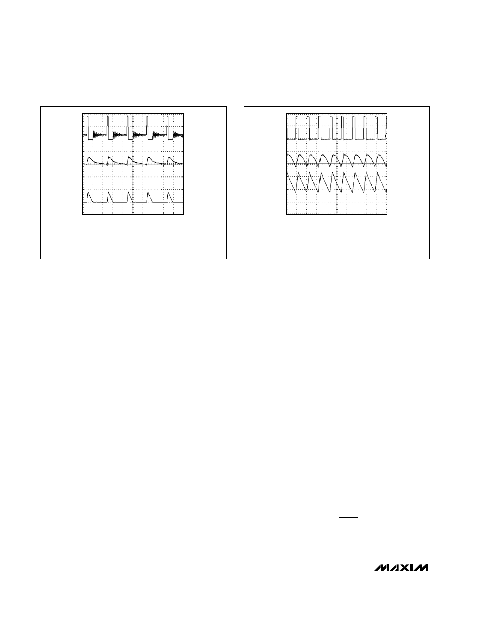
CIRCUIT OF FIGURE 1, V
IN
= 18V, V
OUT
= 3.3V, I
LOAD
= 100mA
A: MOSFET DRAIN, 10V/div
B: OUT, 50mV/div, 3.3V DC OFFSET
C: INDUCTOR CURRENT, 1A/div
A
C
B
10µs/div
Figure 3. Discontinuous-Conduction Mode, Light-Load-Current
Waveform
CIRCUIT OF FIGURE 1, V
IN
= 18V, V
OUT
= 3.3V, I
LOAD
= 1.5A
A: MOSFET DRAIN, 10V/div
B: OUT, 50mV/div, 3.3V DC OFFSET
C: INDUCTOR CURRENT, 1A/div
A
C
B
10µs/div
Figure 4. Continuous-Conduction Mode, Heavy-Load-Current
Waveform
