Chip information, Pin configuration – Rainbow Electronics MAX1538 User Manual
Page 20
MAX1538
Power-Source Selector for
Dual-Battery Systems
20
______________________________________________________________________________________
where V
BAT__MIN
is the minimum battery voltage,
I
CHG_MAX
is the maximum charge current, and L
BAT_
is
the battery’s inductance. C
BAT_
values of 0.01µF are
adequate for typical applications. Adding capacitance
at BAT_ pins lengthens the time needed to detect bat-
tery removal. See the Battery-Absence-Detection Delay
section.
Adapter Removal Debouncing
Upon adapter removal the adapter’s connector may
bounce. To avoid false detection of adapter reinsertion
select R1, R2, and R3 according to the following equation:
where V
Adapter
is the AC-adapter voltage when remov-
ing an AC adapter and airline-adapter voltage when
removing an airline adapter, C
ADPIN
is the capacitance
at ADPIN, and t
Bounce
is the 5ms debounce time. See
the Airline Mode and AC Adapter section for a defini-
tion of V
_Threshold
.
Battery-Absence-Detection Delay
When a selected battery is removed, the system load
quickly pulls BAT_ below 5 x V
MINV_
and another
source is selected. The battery is considered present
and undervoltage until V
BAT_
falls below 2V. Although
another power source is quickly switched to the system
load, capacitance at BAT_ (see the Inductive "Kick"
section) delays the detection of the removed battery. If
another battery is inserted before this delay has
passed, it is considered undervoltage. Calculate the
delay using the following equation:
where I
BAT_
is the 3.9µA BAT_ quiescent current (due to
a 5MΩ internal resistor), and C
BAT_
is the capacitance
from BAT_ to GND. When C
BAT_
= 1µF, t
Absence_delay
corresponds to a 5s time constant. If this time is unac-
ceptable, use a smaller capacitance or connect a resis-
tor or current sink from BAT_ to GND.
Layout
The MAX1538 selector fits in a very small layout.
Ensure that C1 is placed close to V
DD
and GND.
Connect the paddle to GND directly under the IC. A
complete layout example is shown in Figure 10.
Because BATA and BATB are high-impedance nodes,
prevent leakage current between BATA/BATB and
other high-voltage sources by carefully routing traces.
Note that flux remaining on the board can significantly
contribute to leakage current. See the Leakage Current
into BAT_ section.
Minimize parasitic inductance in the BATA and BATB
path to reduce inductive kick during battery discon-
nect. This reduces the capacitance requirement at
BATA and BATB.
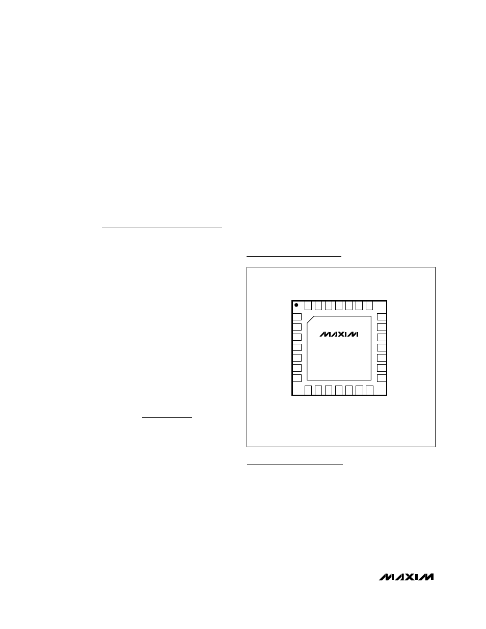
Chip Information
TRANSISTOR COUNT: 5431
PROCESS: BiCMOS
t
V
C
I
Absence delay
BAT
BAT
_
_
=
×
19
R
R
R
V
t
C
V
V
Threshold
Bounce
ADPIN
Adapter
Threshold
1
2
3
_
_
+
+
<
Ч
Ч
−
(
)
28 27 26 25 24 23 22
21
20
19
18
17
16
15
8
9
10 11 12 13 14
1
2
3
4
5
6
7
V
DD
GND
BA
TSUP
B
ATA
DISA
DISB
BA
TB
MINVA
MINVB
BATSEL
RELRN
CHRG
OUT0
OUT1
OUT2
ACDET
AIRDET
ADPIN
ADPPWR
REVBLK
ADPBLK
N.C.
CHGB
CHGA
DISBAT
CHGIN
EXTLD
N.C.
MAX1538 *
THIN QFN
(5mm x 5mm)
*EXPOSED PADDLE
Pin Configuration