Bypassing and board layout, Chip information – Rainbow Electronics MAX1426 User Manual
Page 14
MAX1426
10-Bit, 10Msps ADC
14
______________________________________________________________________________________
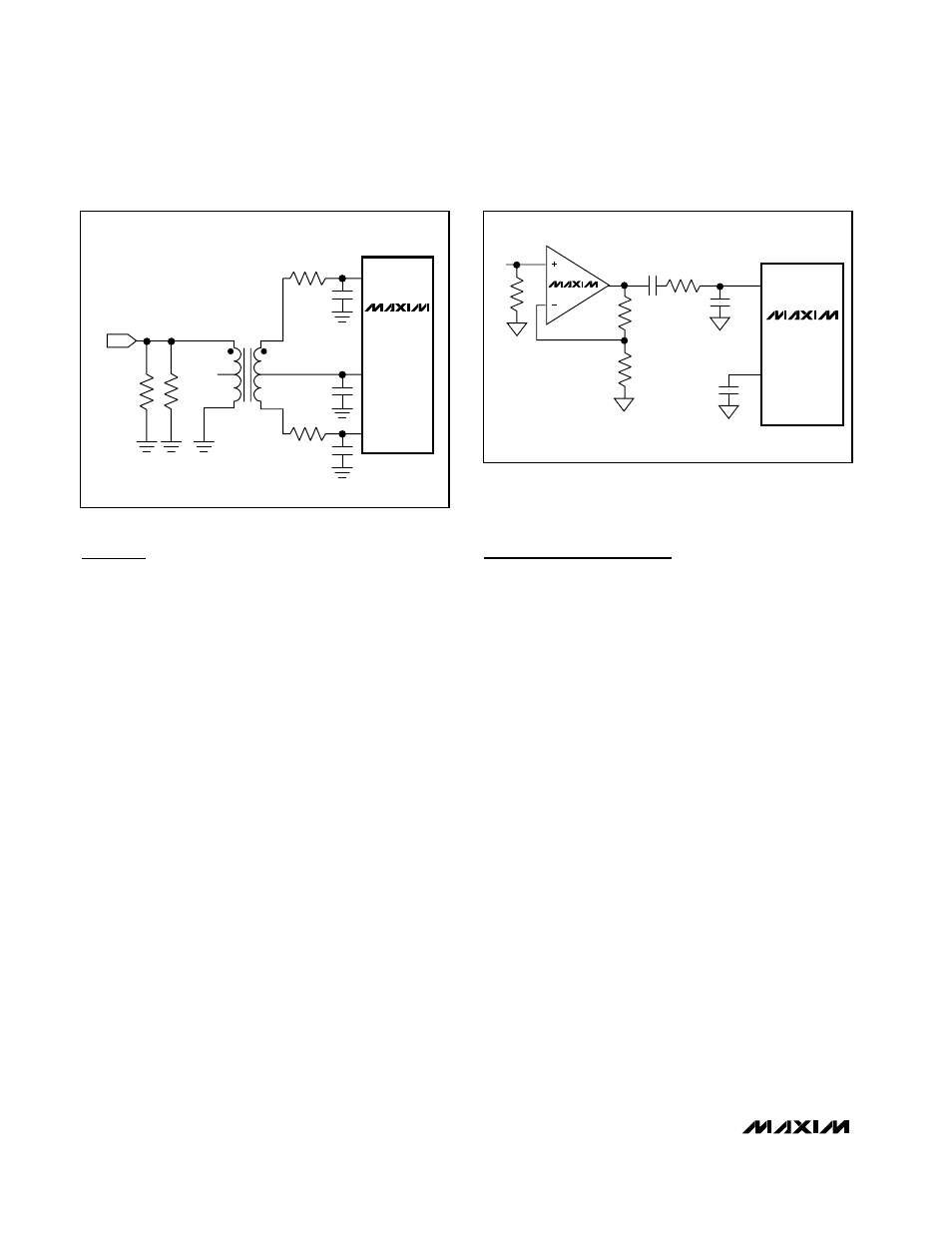
Bypassing and Board Layout
The MAX1426 requires high-speed board layout design
techniques. Locate all bypass capacitors as close to
the device as possible, using surface-mount devices
for minimum inductance. Bypass all analog voltages
(AV
DD
, REFIN, REFP, REFN, and CML) to AGND.
Bypass the digital supply (DV
DD
) to DGND. Multilayer
boards with separated ground and power planes pro-
duce the highest level of signal integrity. Route high-
speed digital signal traces away from sensitive analog
traces. Matching impedance, especially for the input
clock generator, may reduce reflections, thus providing
less jitter in the system. For optimum results, use low-
distortion complementary components such as the
MAX4108.
Figure 8. Using a Transformer for AC-Coupling
Figure 9. Single-Ended AC-Coupled Input Signal
MAX1426
T1
N.C.
IN1
6
1
5
2
4
3
C3
22pF
C9
22pF
0.1
µF
R2
100
Ω
R3
100
Ω
R5
25
Ω
R4
25
Ω
MINICIRCUITS
KKB1
INP
CML
INN
MAX1426
0.1
µF
100
Ω
50
Ω
±2V
100
Ω
22pF
INP
INN
0.1
µF 50Ω
V
IN
±V
MAX4108
TRANSISTOR COUNT: 5305
Chip Information