Analog inputs (inp, inn), On-chip reference circuit – Rainbow Electronics MAX1123 User Manual
Page 11
Analog Inputs (INP, INN)
INP and INN are the fully differential inputs of the
MAX1123. Differential inputs usually feature good rejec-
tion of even-order harmonics, which allows for enhanced
AC performance as the signals are progressing through
the analog stages. The MAX1123 analog inputs are self-
biased at a common-mode voltage of 1.4V and allow a
differential input voltage swing of 1.25V
P-P
. Both inputs
are self-biased through 2.2kΩ resistors, resulting in a
typical differential input resistance of 4.4kΩ. It is recom-
mended to drive the analog inputs of the MAX1123 in
AC-coupled configuration to achieve best dynamic per-
formance. See the AC-Coupled Analog Inputs section for
a detailed discussion of this configuration.
On-Chip Reference Circuit
The MAX1123 features an internal 1.23V bandgap ref-
erence circuit (Figure 3), which, in combination with an
internal reference-scaling amplifier, determines the full-
scale range of the MAX1123. Bypass REFIO with a
0.1µF capacitor to AGND. To compensate for gain
errors or increase the ADC’s full-scale range, the volt-
age of this bandgap reference can be indirectly adjust-
ed by adding an external resistor (e.g., 100kΩ trim
potentiometer) between REFADJ and AGND or
REFADJ and REFIO. See the Applications Information
section for a detailed description of this process.
MAX1123
1.8V, 10-Bit, 210Msps Analog-to-Digital Converter
with LVDS Outputs for Wideband Applications
______________________________________________________________________________________
11
INP
INN
D0P/N–D9P/N
ORP/N
CLKP
CLKN
t
CH
t
CL
DCLKP
DCLKN
N - 8
N - 7
N
N + 1
t
PDL
N - 7
N - 8
N
N + 1
N
N + 1
N + 8
N + 9
t
CPDL
t
LATENCY
t
AD
N - 1
SAMPLING EVENT
SAMPLING EVENT
SAMPLING EVENT
SAMPLING EVENT
t
CPDL
- t
PDL
t
CPDL
- t
PDL
~ 0.4 x t
SAMPLE
with t
SAMPLE
= 1/f
SAMPLE
NOTE: THE ADC SAMPLES ON THE RISING EDGE OF CLKP. THE RISING EDGE OF DCLKP CAN BE USED TO EXTERNALLY LATCH THE OUTPUT DATA.
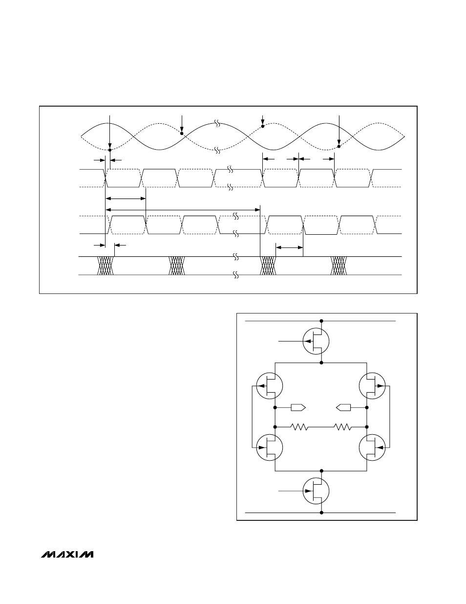
Figure 4. System and Output Timing Diagram
OV
CC
OGND
2.2kΩ
2.2kΩ
V
OP
V
ON
Figure 5. Simplified LVDS Output Architecture